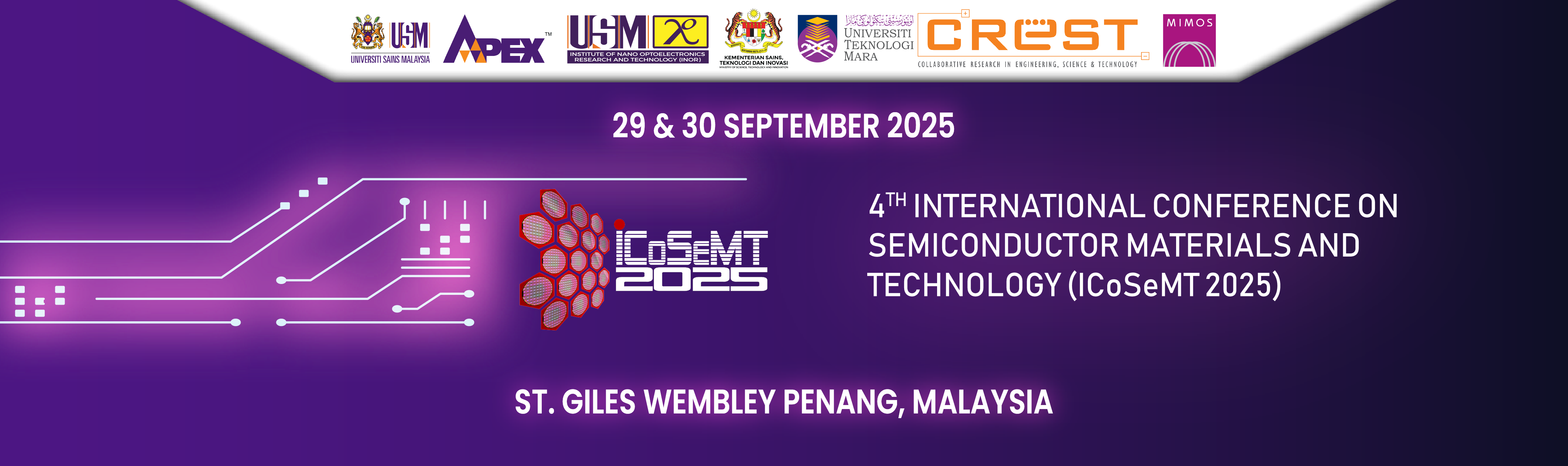
ABOUT ICoSeMT
4th International Conference on Semiconductor Materials and Technology (4th ICoSeMT 2025) is a biennial event that is jointly organized by Institute of Nano Optoelectronics Research and Technology (INOR), Universiti Sains Malaysia (USM), Universiti Teknologi MARA Cawangan Pulau Pinang (UiTMCPP), National Nanotechnology Centre (NNC), Ministry of Science, Technology and Innovation of Malaysia (MOSTI), MIMOS Berhad and Collaborative Research in Engineering, Science & Technology (CREST) with the Theme “Innovation Towards A Sustainable Tomorrow”. The primary focus of the conference is to create an effective medium for institutions and industries to share ideas, knowledge, and expertise in the fields related to Semiconductor Materials and Technology.
This year, with the aim to promote positive innovation culture and encourage innovation activities and from different walks of life, a sub-event entitled International Invention, Innovation & Design Expo (INoDEx 2025) is going to be held concurrently. This sub-event will be a great platform in creating opportunities for local and international participants to present their innovations and inventions. Eventually, both events will lead to interaction and future collaboration among the local and international participants.
CONFERENCE SCHEDULE
Registration of guests and participants will take place on 29 September 2025, from 7:30 AM to 9:00 AM, at Level 10. To gain access to all sessions, as well as lunch, coffee breaks, and tea breaks, it is mandatory to possess a badge. Please ensure that your badge is always kept with you, except during the dinner event. For those who have chosen to attend the dinner, a coupon will be provided during the registration process. Please note that individuals are not permitted to collect badges on behalf of other participants.
Conference Cancellation Policy: No refunds will be granted.
AWARD:
Call for Paper
"We are pleased to inform conference participants that we are partnering with Trans Tech Publications Ltd as our publishing partner to welcome submission of full papers for consideration of publication in Scopus-Indexed Proceedings following the review process in journals managed by Trans Tech Publications Ltd on the platform https://www.scientific.net/.
The Scientific Committee will conduct a peer review of the papers. Each submitted manuscript will undergo evaluation by a minimum of two independent reviewers (single-blind peer-review process). Manuscripts that receive acceptance based on the reviews will be forwarded for evaluation by the publisher through the conference committee. The appropriate journal for the accepted manuscript will be identified in collaboration with both the publisher and the conference committee. The submitted manuscripts must not have been previously published elsewhere. The average length of the Paper is to be 6 pages.
Click button below to register and upload your abstract and full paper.
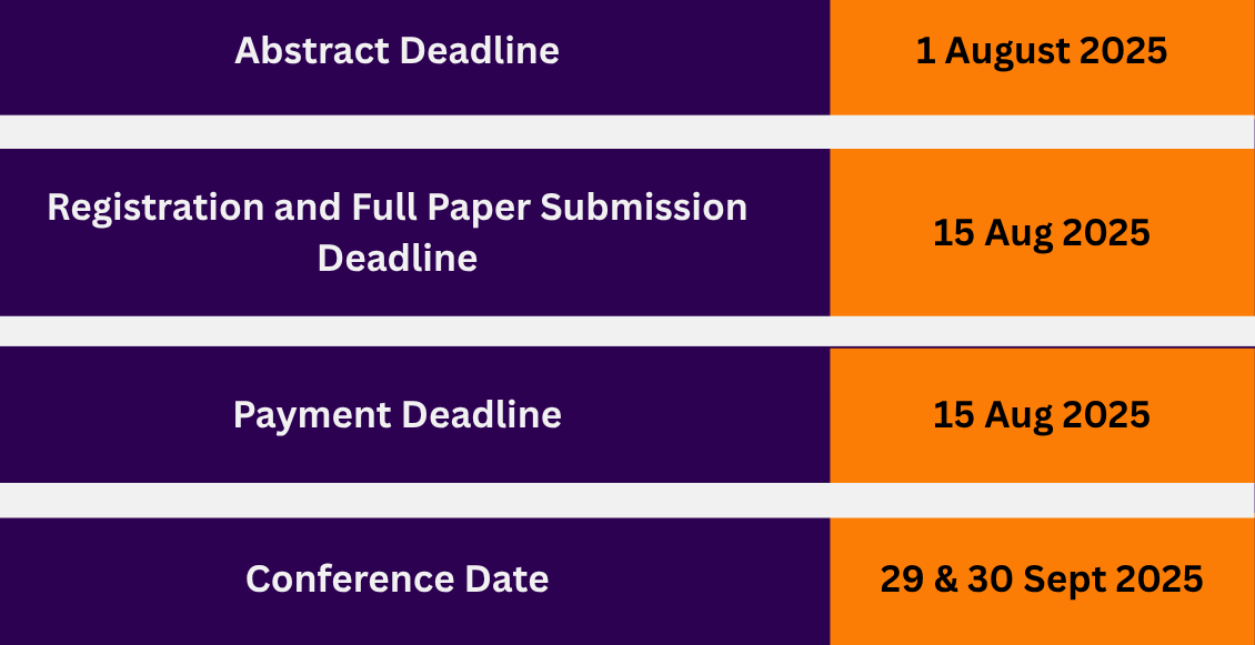
IMPORTANT DATES [update]
KEYNOTE SPEAKERS

He currently holds the position of Senior Director and Head of Wide-Band-Gap Semiconductor R&D at Infineon Technologies (Kulim) Malaysia, where he is leading the research and development efforts in the wide-band-gap semiconductor field, driving innovative solutions and technological advancements.
His technical knowledge spans a variety of technology platforms, including DRAM/Flash Memory, Power Discrete, MEMS/Sensors, and Wide-Band-Gap technologies. With an M.Sc. in Material Science & Engineering from the National University of Singapore. Sim is passionate about mentoring emerging leaders in the field and fostering collaboration, drawing from his extensive international experience.
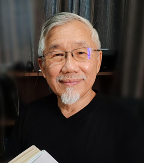
- Co-creating IrDA (an infrared wireless standard which resulted in 2B+ devices and inspired PayPal & Bluetooth)
- Pioneering the DAT/DDS storage system with Sony (and created a new $600M market)
- Developing the world’s first data-encrypted HDD at Seagate
- Advancing Silicon Photonics, DNA chips & MEMS as SilTerra VP
- Bridging industry-workforce gaps as CEO of Penang Skills Development Centre
- Driving national semiconductor strategy as MIMOS Board Membe
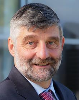
Since 4/92 he is Head of the Materials Technology Department at Ferdinand-Braun-Institut gGmbH, Leibniz-Institut fuer Hoechstfrequenztechnik (FBH) in Berlin,Germany. Since 6/2014 he is adjunct Professor at TU Berlin where he teaches Applied Physics.
His research interests include MOVPE growth of GaAs-based laser structures as edge emitters and VCSELs, GaN-based lasers, as well as AlGaN LEDs and transistor structures. He has authored and co-authored around 530 scientific papers and 6 book chapters on growth studies as well as device growth in MOVPE, MOMBE and HVPE. He has served as Associate Editor for J. Crystal Growth and IEEE Photonics Letters and as reviewer for numerous journals and research funding agencies.
1999 he founded the epiwafer foundry Three-Five Epitaxial Services AG (TESAG) which he headed until the end of 2008. In 1999 he also co-founded LayTec GmbH (now LayTec AG), a producer of in-situ metrology tools for MOVPE. He was Head of the Supervisory Board of LayTec AG 2011 - 2017.
He won a Japan IBM Science Prize in Electronics in 2010, an Ichimura Science Prize in 2011, a Science and Technology Award from the Minister of Education, Culture, Science and Technology in 2014, a Compound Semiconductor Electronics Achievement Award (Prof. Isamu Akasaki Award) of The Japan Society of Applied Physics in 2019, etc. His research focuses on crystal growth of AlGaN/AlN nitride-semiconductors and development of deep-UV LEDs. He is also developing terahertz quantum cascade lasers (THz-QCLs).
PLENARY SPEAKER
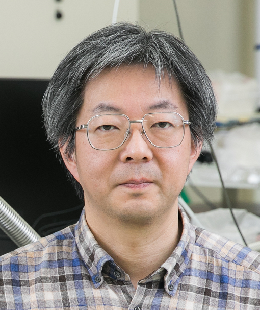
RIKEN Institute, Japan
Later he joined the team of FUTURE Photovoltaic (PV)-Innovation, Japan Science and Technology Agency, Fukushima Renewable Energy AIST (FREA), Koriyama in 2014. In 2017, he moved to Riken (RAP) as a SPDR and later in 2020 he moved to RIKEN Pioneering Research Institute (PRI) as a research scientist (Prof. H. Hirayama Lab). Since then, he has been doing research on the epitaxial growth, characterization, and device applications of group III-nitride semiconductor-based UV LEDs and UV Laser Diodes. He has developed a world first AlGaN UVB LED with a world record efficiency of 9.6% with a light power of 40 mW on the wafer (Sci Rep 12, 2591 (2022)).
Presently, he is working as a senior research scientist at Riken and working on the project of far-UVC LEDs for SARS-CoV-2 (Corona Virus) inactivation. He reported the world shortest 228nm far-UVC LED grown on a low-cost c-Sapphire with EQE of 0.32% (Phys. Status Solidi (A) 221, 2400064 (2024)). He bears various roles and responsibilities, such as a renowned member of the Japan Society of Applied Physics (JSAP), and guest editor of several journals. He received several national and international awards for his invention of Boron-doped BaSi2 Solar cells and AlGaN-based UVB LEDs. He delivered more than 150 talks including keynote and invited talks both in the local as well as in the international conferences. He is the author and co-author of more than 110 pre-reviewed research publications.
He has been based in Malaysia since 2001 and is currently President of SFAM - the Semiconductor Fabrication Association of Malaysia. He was one of the exco committee members involved in the earlier phase of conceptualisation and inception of CREST since March 2012. Dr. Lacey was bestowed with an honorary Doctor of Science by Universiti Sains Malaysia at the Arau Palace in 2021, an accolade reflecting his profound impact on advancing LED technologies and expanding opportunities in Malaysia.
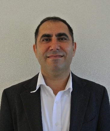
Dr. Sideq’s expertise in innovation, intellectual property, and strategic partnerships continues to shape Malaysia’s semiconductor and advanced manufacturing ecosystem.

Within the Research Center on Hetero-Epitaxy & Applications (CRHEA), since 2004, he has been working on semiconductor materials with very large band gaps, in particular gallium and aluminum nitride alloys (AlGaN), for the production of optoelectronic components (light-emitting diodes (LEDs), lasers, optical waveguides, etc.). His work has led him to participate in numerous French National Research Agency (ANR) projects, as well as European projects. In particular, he has been coordinating ANR projects on white LEDs and UV LEDs, and within the Labex GaNEX, - national network on GaN-based materials -, on materials for UV emission. He is currently responsible for a project in partnership with the RIBER SA Company, a leader in the field of molecular beam epitaxy components. He is the author/co-author of over 140 publications and five patents.
He is responsible for the Advanced Photonics Group in CRHEA. He is also a member of the Environmental and Health Sciences (SENS) team, where he is developing the UV LED theme, and of the 2D+ team, where he is developing the van der Waals epitaxy growth of AlGaN materials on 2D materials (h-BN and graphene). He is a member of the Board of Directors since 2018 and of the Laboratory Council since 2016. He is involved in the Côte d'Azur University as a lecturer in electronics at the "Networks and Telecommunications" Institute of Technology, and as a member of the scientific council of "Complex Systems" Academy of Excellence. He is (has been) involved as a member of numerous program and expert committees in major international conferences on nitrides (ICNS, IWN, ISGN), ultra-wide bandgap materials (IWUMD) and semiconductor components and materials (SSDM - Japan). He is a visiting Professor at the Far Infra-Red (FIR) Center of the University of Fukui, Japan, since 2019.
SilTerra Malaysia Sdn. Bhd
He graduated with Bachelor of Science in Electrical and Electronic from The Robert Gorden University, Aberdeen, United Kingdom and obtained a full scholarship from ODASS to further his Master of Science (MSc) in Microelectronics and Information System from Liverpool John Moores University, United Kingdom. He has more than 30 years of semiconductor experience. Prior to join SilTerra, he was attached with multi-national companies such as Komag Corporation, INTEL Corporation, Akashi Kuboto Corporation (pioneer start-up team) and Showa Aluminium Corporation (pioneer start-up team).
He also has passion and interest in research for continues improvement in optimizing the wafer fabrication process. He has filed in multi publications within the companies, journal, national and international conferences.
In recognition of his experienced, he has given the opportunity as the project leader for the technologies outsourcing, transfer and wafer fabrication consultant. He managed transfer multi new technologies from beginning to mass production within 9 months’ time prior.
Her work focuses on translating scientific innovation into national economic value, particularly within the semiconductor sector. Azimah has led strategic initiatives that position Malaysia competitively in the global semiconductor value chain, including:
- Developing investment strategies for the MIMOS Semiconductor Technology Center, enabling Malaysia’s emergence as a MEMS supply chain player.
- Advising on semiconductor ecosystem development in Uzbekistan, fostering regional collaboration.
- Launching My-AI, Malaysia’s national AI data-sharing platform to support high-performance computing and research commercialization.
Azimah’s expertise spans IP valuation, patent analytics, licensing, and market intelligence—tools she uses to assess technology readiness and economic viability. Her strategic models have guided commercialization of indigenous technologies across sectors such as healthcare, education, and finance.
She is a co-inventor of eight patents and the architect of e-IPMS, an IP management system that elevated MIMOS’s global patent rankings. Her contributions earned recognition including the National Best Trademark Award and top rankings in the PCT Yearly Review.
Academically, Azimah holds a Master’s in Intellectual Property Law and a professional degree from the Institute of Chartered Secretaries and Administrators (ICSA). She is professionally trained by the Japan Patent Office, JIII/AOTS, and MyIPO in strategic IP and valuation.
As a HRDF-certified corporate trainer, she speaks regularly at international forums including WIPO, USPTO, and IPBC Asia, and collaborates with global partners such as Clarivate UK. She also serves as an Adjunct Professor at the Malaysian-Japan International Institute of Technology (UTM).
In her plenary session at ICoSeMT 2025, Azimah will present a strategic framework to stratify semiconductor innovations—such as III-nitride materials and wide bandgap semiconductors—based on their economic impact, market readiness, and cross-sectoral potential, offering actionable insights for regional stakeholders to align research excellence with national development goals.
Prof. Tao has published more than 70 papers, including Nature Nanotechnology, Advanced Functional Materials, IEEE Electron Device Letters etc. He was elected as Young Scholar of Changjiang River from Ministry of Education, China.
INVITED SPEAKER
Universiti Sains Malaysia (USM)
He was invited as a keynote speaker at major conferences, including the International Laser Technology and Optics Symposium (ILATOS 2015) and the 4th MAHSA International Conference on Advances in Life Science and Engineering (MI-CALSE 2024). He also serves as a reviewer for the EURIZON Fellowship Programme and is a multiple award winner in innovation competitions.
At the Institute of Nano Optoelectronics Research and Technology (INOR), he leads a sub-project on III-nitrides nanophotonics under the Higher Institution Centre of Excellence (HiCOE) program and actively teaches postgraduate courses in solid-state physics and nanomaterials. He is a member of the Malaysian Solid State Science and Technology Society (MASS) and Optica (formerly the Optical Society of America).
Dr. Yilmaz Dikme is the Technical Director and of co-founder ELEMENT 3-5 GmbH, Germany. He received his Ph.D. degree from RWTH Aachen University, Germany and has more than 20 years of experience in the field of group III-nitride material deposition by MOCVD and by plasma. At ELEMENT 3-5 he has developed and patented a epitaxial process called Next Level Epitaxy that allows the growth of AlN, SiC and Diamond at low temperatures with high throughput. He has co-authored more than 50 scientific publications.
Mohd Hanapiah Abdullah is a distinguished senior lecturer at Universiti Teknologi MARA (UiTM), Department of Electrical and Electronic Engineering, specializing in nanotechnology, nanomaterials, and dye-sensitized solar cells. With a deep passion for advancing sustainable energy solutions, his expertise lies in the development and application of cutting-edge nanomaterials to enhance the efficiency and performance of solar energy systems.
A dedicated researcher and academic who aim himself to the field of nanoscience, focusing on material innovation and functional applications in renewable energy. His work emphasizes photovoltaic advancements, particularly in the field of dye additive for organic based dye-sensitized solar cells, aiming to push the boundaries of energy conversion efficiency.
Beyond academia, he is a recognized member of the Board of Engineers Malaysia (BEM), underscoring his commitment to professional engineering excellence. His affiliation with BEM reflects his active participation in engineering standards, research collaboration, and technological development that bridge academic research with industry applications.
Driven by a vision to foster interdisciplinary partnerships, he actively seeks collaborations with various stakeholders, including industry leaders, research institutions, and technology innovators. His goal is to build synergies that accelerate breakthroughs in nanotechnology and sustainable energy, ensuring impactful solutions for global challenges.
With a steadfast commitment to scientific advancement and collaborative innovation, Mohd Hanapiah Abdullah continues to inspire research excellence, mentor future scientists, and contribute to the global pursuit of sustainable technology.
Mr. Allen Cheah
Allen Cheah has over 25 years of experience working in both ODM/OEM and EMS R&D, as well as Development Engineering fields with a primary focus in Design Engineering & Product Realization for multinational companies in Penang. His last held position was a Senior Director of Asia Design Center, a Regional Development and Application Engineering Role across EU, U.S., Malaysia, China, Taiwan and Thailand for a myriad of customers that spans to DUV/EUV Lithography Equipment stage with ASML.
He has a Dual-Bachelor of Science Degrees in both Electrical Engineering and Mechanical Engineering from the University of Kentucky, Lexington U.S.A. He is a team player for the Malaysia’s National Semiconductor Strategy (NSS) – Advanced Packaging Cluster via CREST Malaysia to support the National Vision, Framework and Technology Envelope for long term spurious growth in Advanced Packaging SIP (System in Package) for Malaysia.

Assoc. Prof. Dr. İlkay Demir is the Director of the Nanophotonic Research and Application Center (CÜNAM) at Sivas Cumhuriyet University, Turkey, a National Research Infrastructure. He earned his Ph.D. in Physics from Sivas Cumhuriyet University, where his research focused on the epitaxial growth and characterization of III–V semiconductor structures for quantum cascade lasers. During his doctoral studies, he was awarded a TÜBİTAK 2214-A scholarship to conduct research at the Center for Quantum Devices, Northwestern University, USA, under the supervision of Prof. Manijeh Razeghi.
With more than 15 years of experience in metal-organic chemical vapor deposition (MOCVD), his expertise spans the growth of III–V and III–nitride semiconductors, including GaN, AlN, AlGaN, InGaAs, and InAlAs, for advanced photonic and optoelectronic devices. His research covers high-quality nitride materials on silicon and sapphire substrates, ultraviolet light-emitting diodes (UV-LEDs), infrared photodetectors, quantum cascade lasers, and gradient-index optical coatings for defense, space, and quantum technologies.
Dr. Demir has coordinated multiple national and international R&D projects, authored over 100 peer-reviewed publications, and has been an invited speaker at international conferences. He actively contributes to European and global semiconductor research networks, fostering collaborations between academia and industry to accelerate innovation in advanced materials and device technologies.
Booth Exhibition Packages


SPONSORSHIP PACKAGES


For more information regarding sponsorship, kindly contact us at the following information:
Assoc. Prof. Dr. Ng Sha Shiong (shashiong@usm.my | +6013-4729700)
Dr. Siti Juliana Abu Bakar (sitijuliana@uitm.edu.my | +6019-4752209)
Opportunities
Learn & Share
Ask Expert
Explore Event
Publish Your Article
Conference Venue

The St Giles Wembley-Premier Hotel, Penang, Malaysia is just a half-hour’s drive to the famed Batu Feringghi beach and is a mere 5 minutes away from the Ferry Terminal. Being even closer to fun and entertainment outlets with transport services readily available from the hotel, you can explore the many wonders and historical attractions of Penang Island to the fullest.Stretigically located in the city of Georgetown, Penang, near to restaurants, hawkers centre, culture, sightseeing area of Penang city, The St Giles Wembley – Premier Hotel, a 4 – Star hotel is only 18.2 kilometers away from Bayan Lepas International Airport.
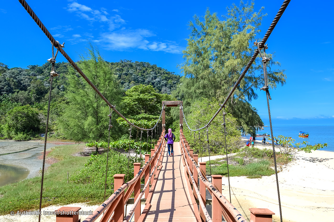
Attraction Places in Penang, Malaysia
Penang National Park
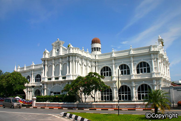
Penang State Museum & Art Gallery
Penang Street Art

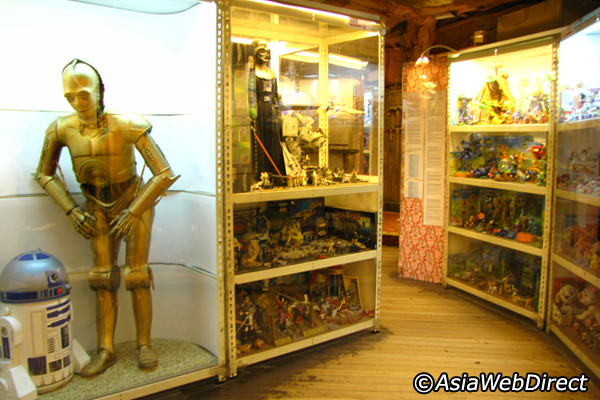
Penang Toy Museum
Penang Hill

Penang War Museum
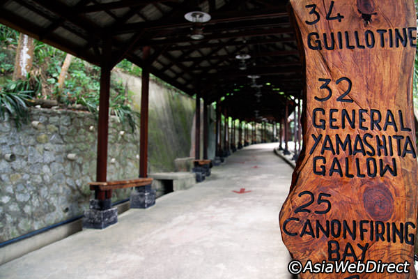
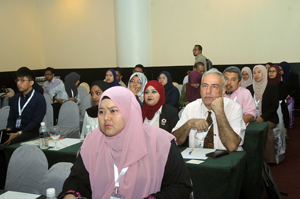
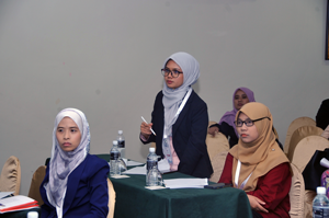
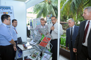
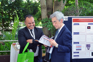
Photo Gallery | ICoSeMT 2023


