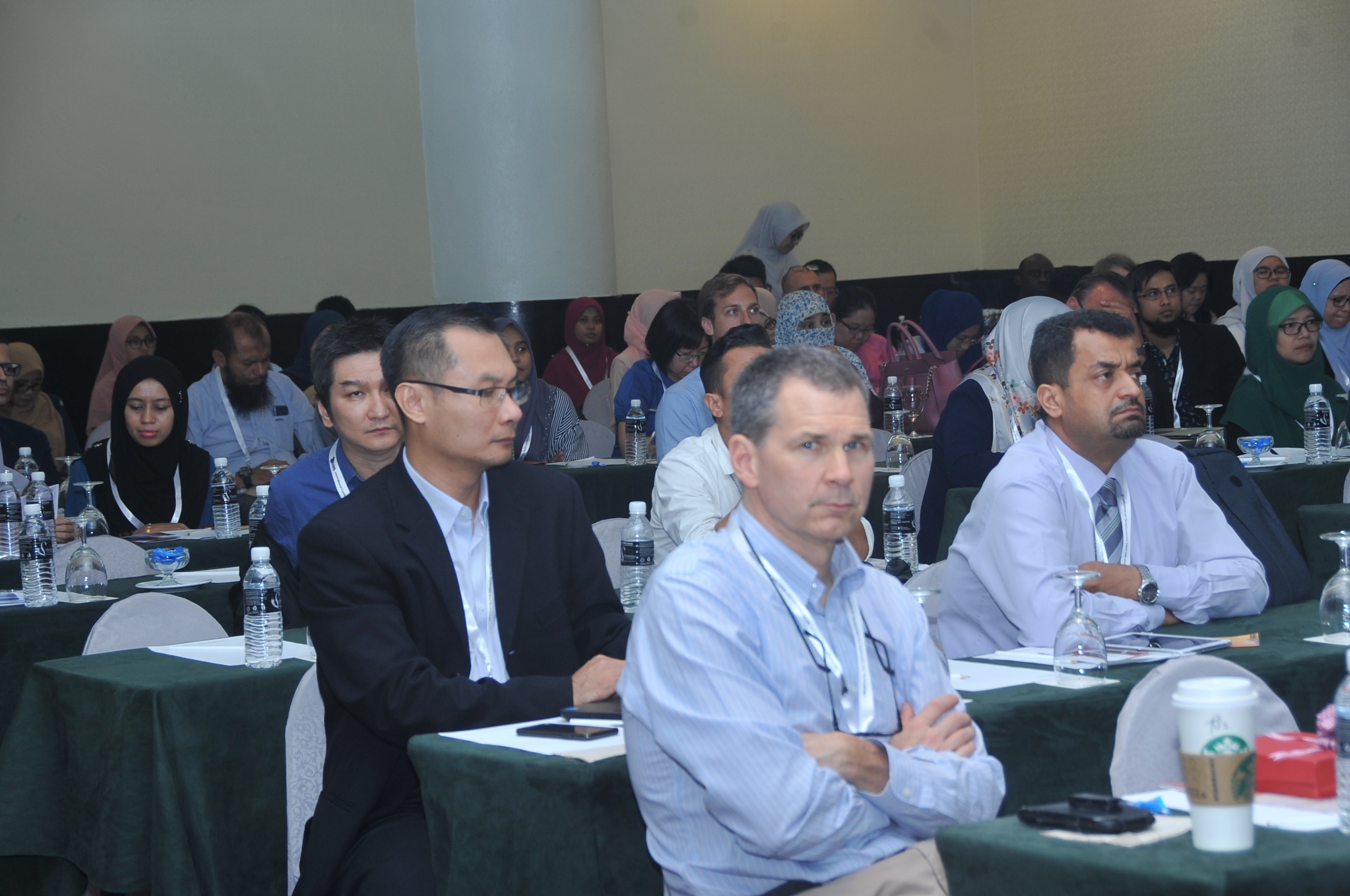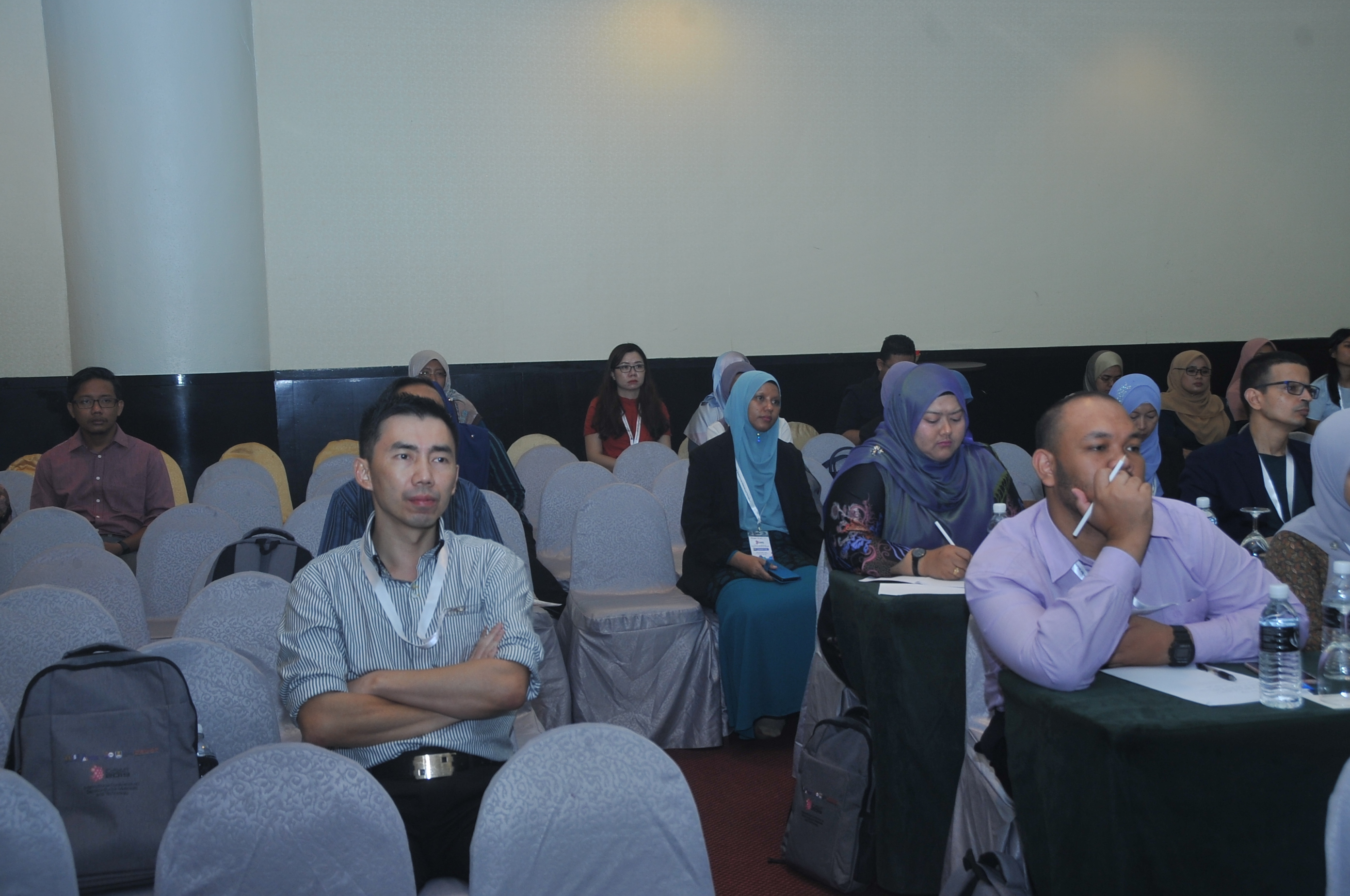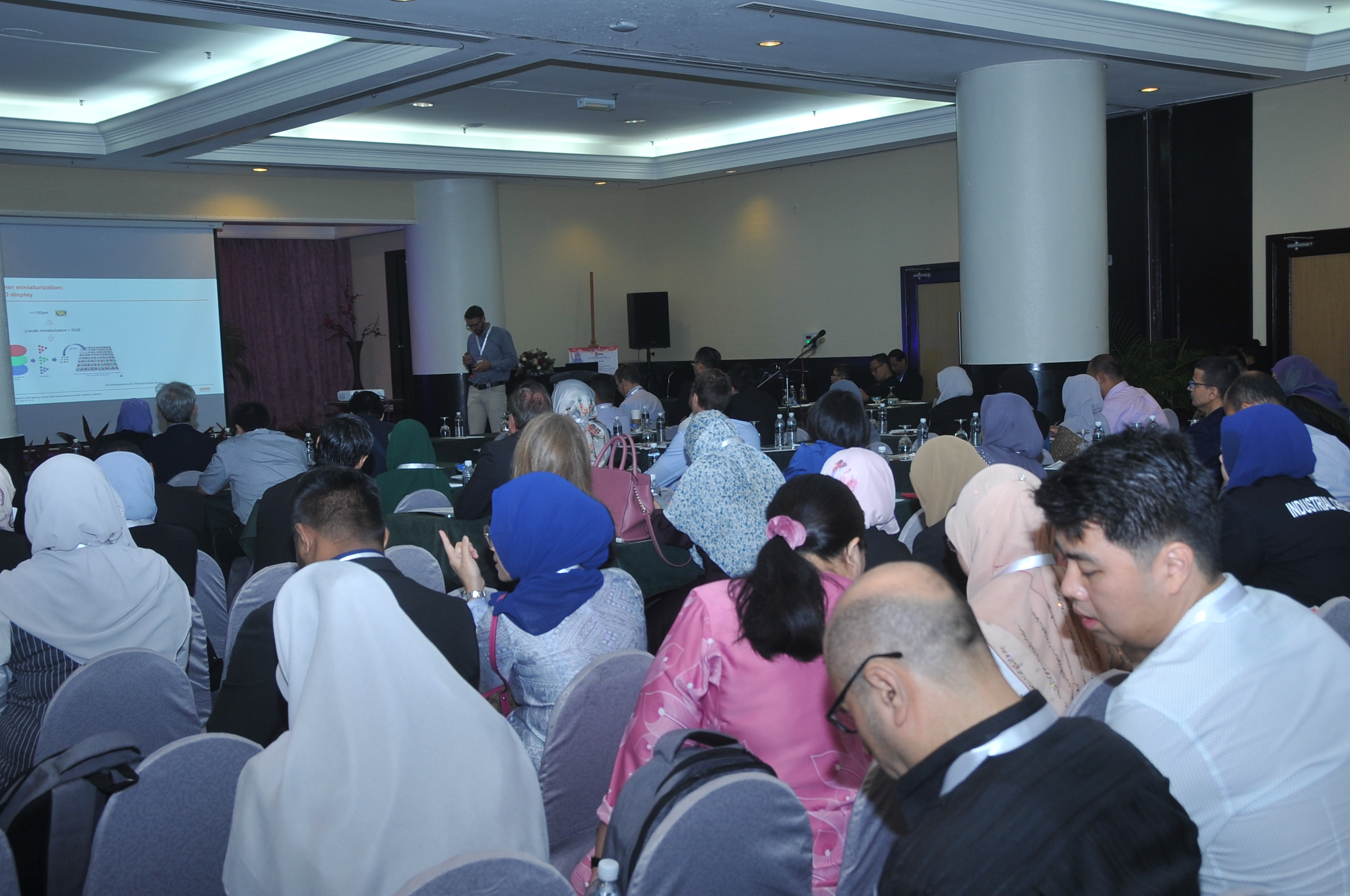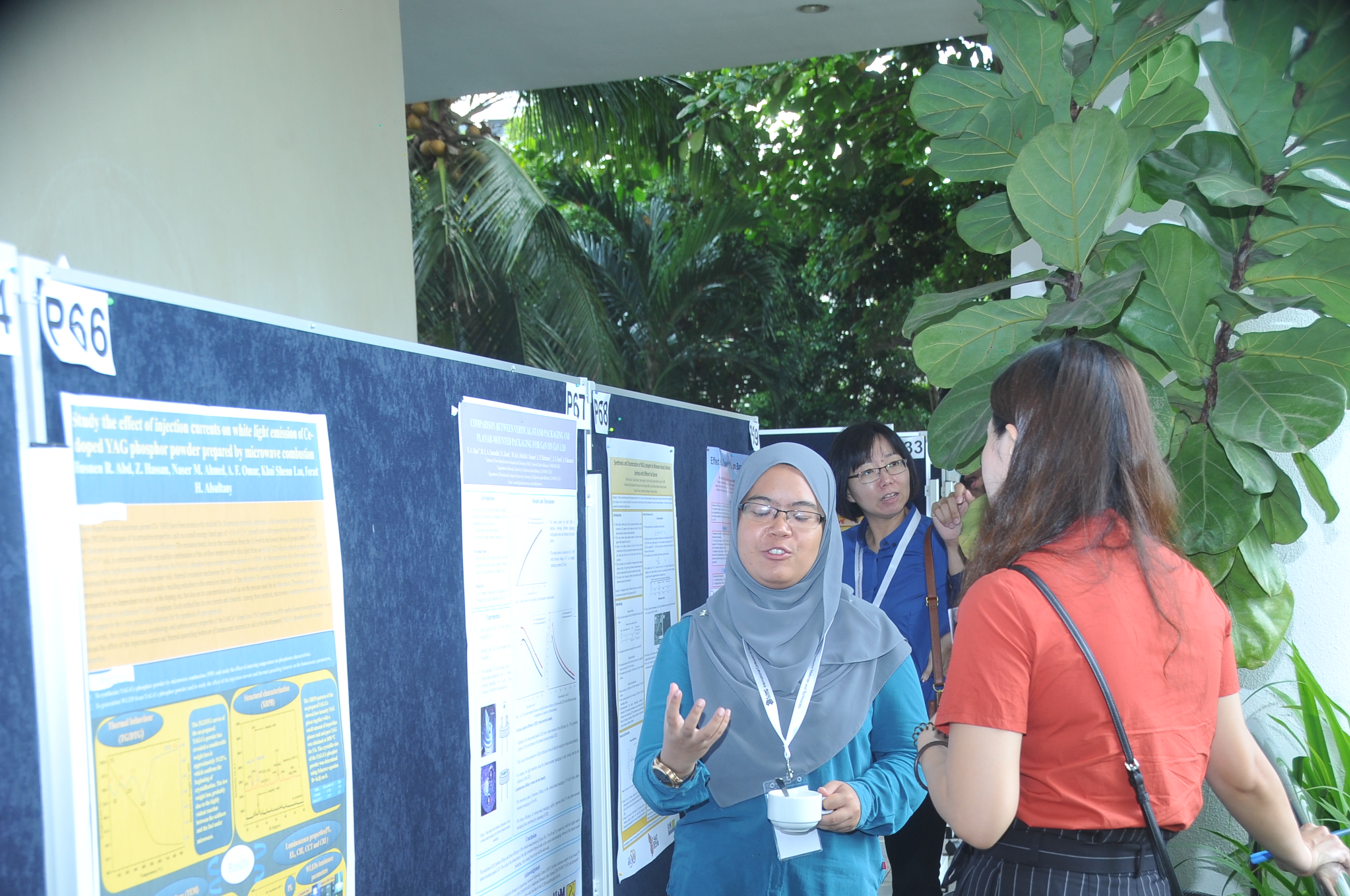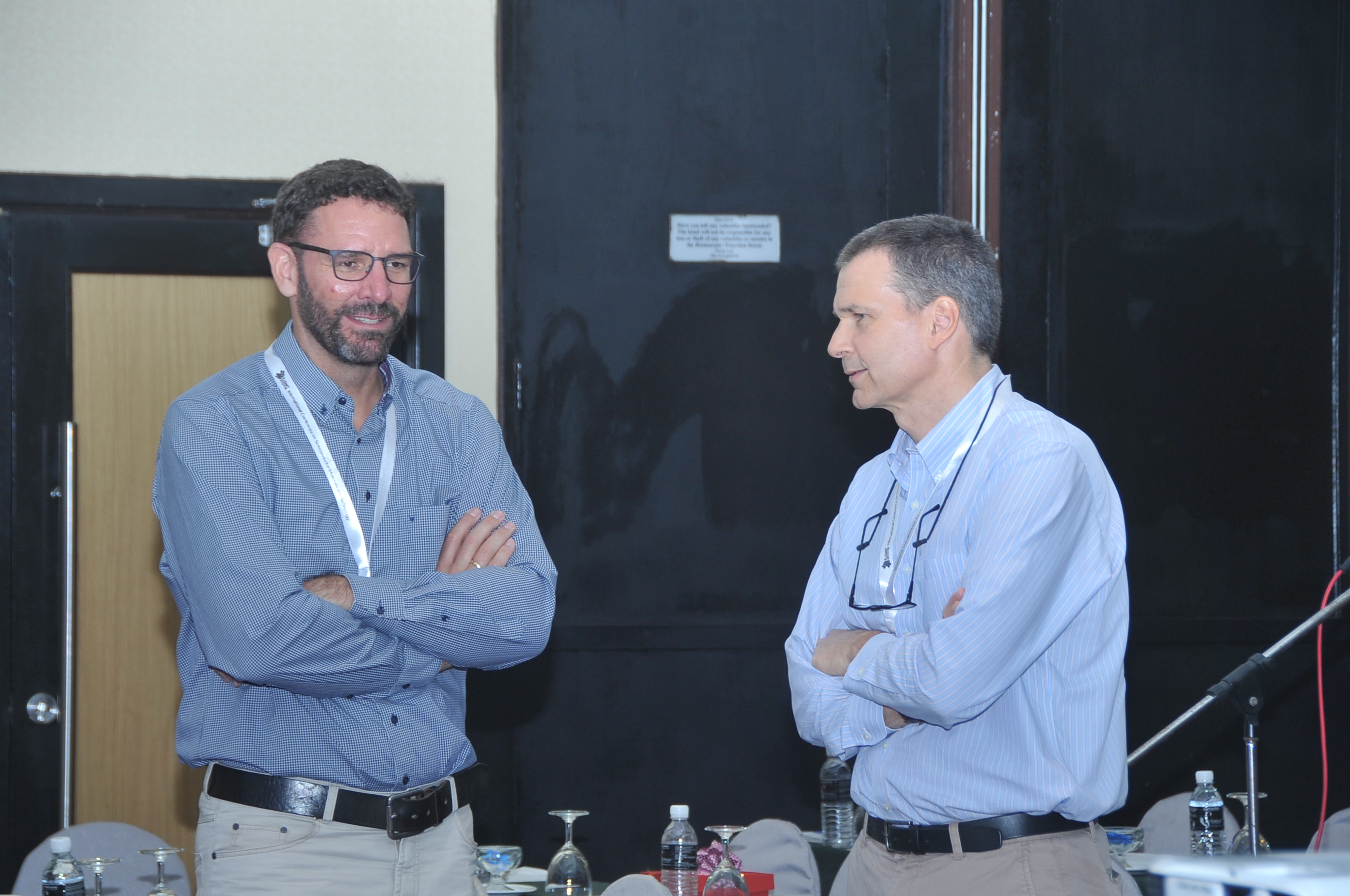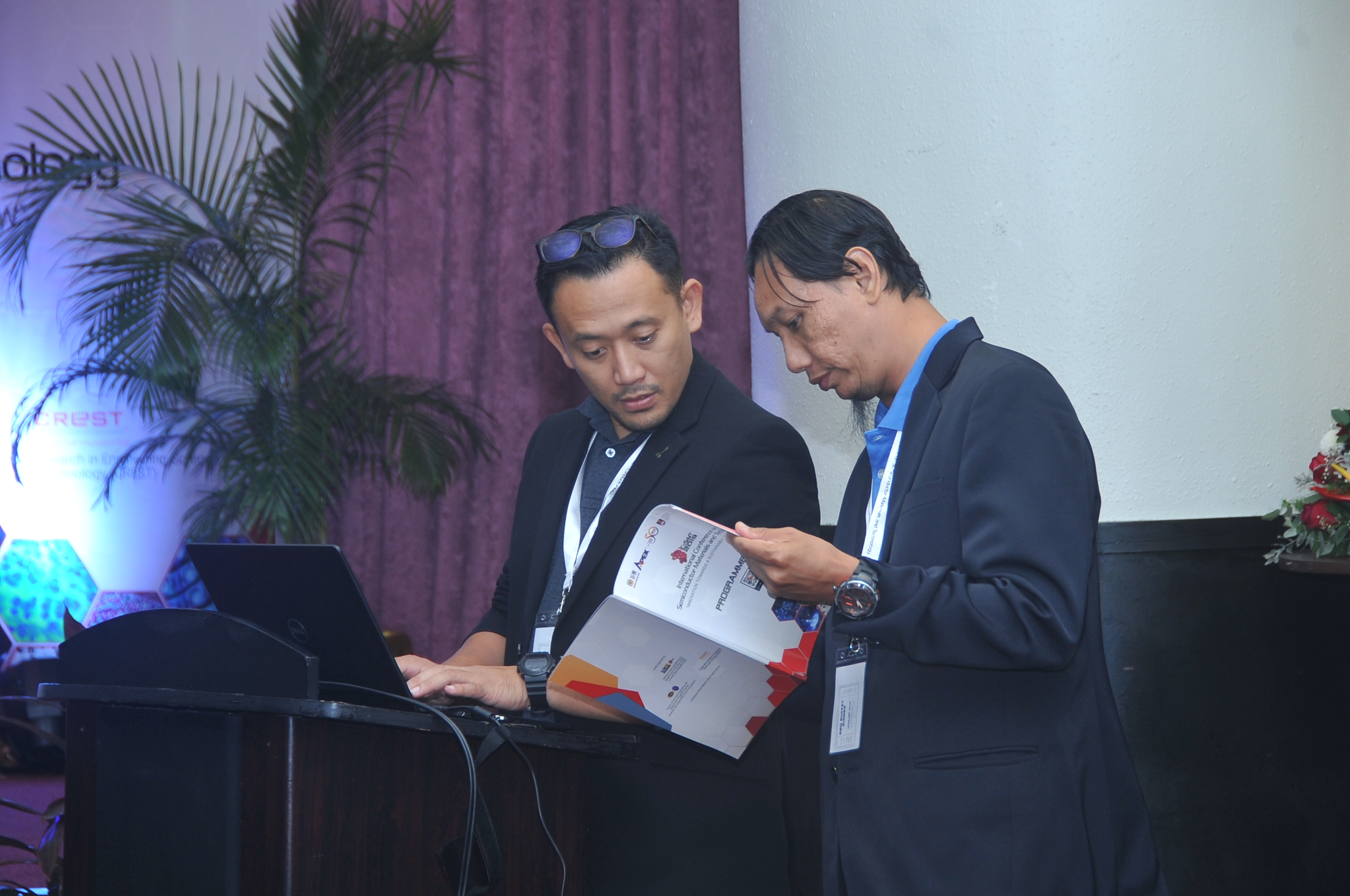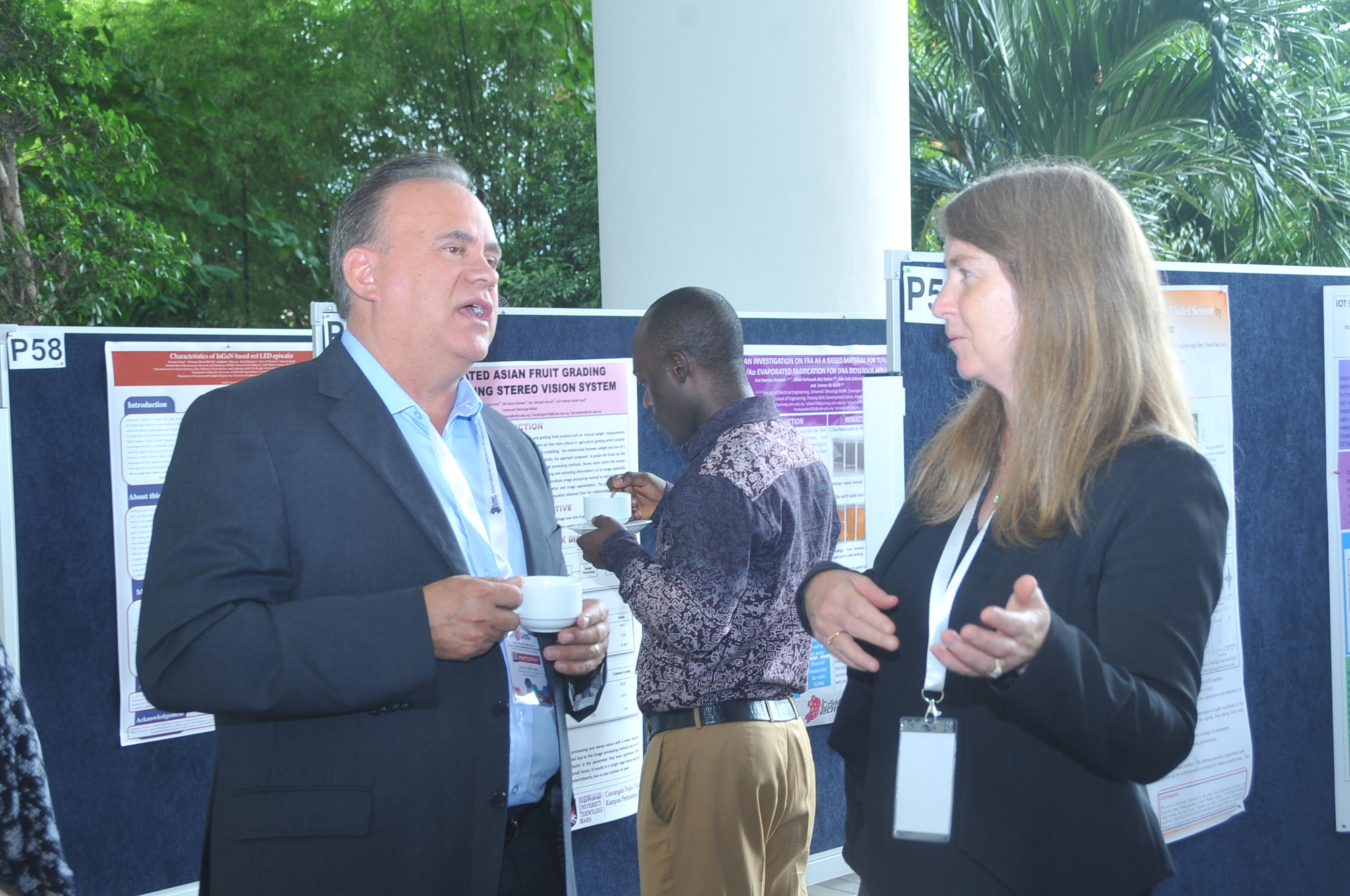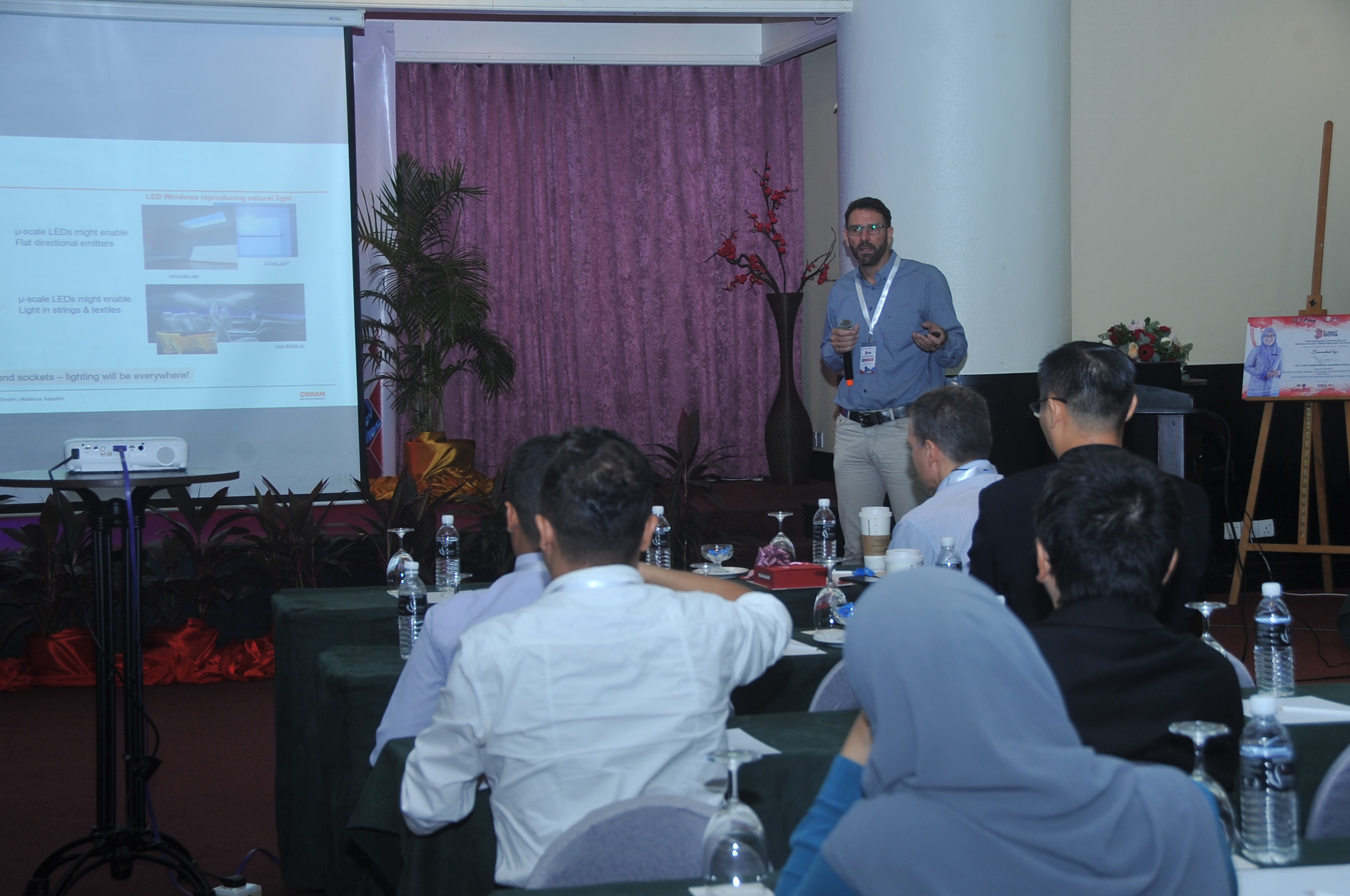
ICoSeMT & INoDEx 2021 Opening Ceremony
ICoSeMT & INoDEx 2021 Closing Ceremony

ABOUT ICoSeMT
2nd International Conference on Semiconductor Materials and Technology (2nd ICoSeMT 2021) is a biennial event that is jointly organized by Institute of Nano Optoelectronics Research and Technology (INOR), Universiti Sains Malaysia (USM), Universiti Teknologi MARA Cawangan Pulau Pinang (UiTMCPP), Collaborative Research in Engineering, Science & Technology (CREST), and Industrial Centre of Innovation in Smart Manufacturing (ICI-SM), SIRIM Industrial Research (SIRIM IR), SIRIM Berhad with the Theme “Innovation Towards A Sustainable Tomorrow”. The primary focus of the conference is to create an effective medium for institutions and industries to share ideas, knowledge, and expertise in the fields related to Semiconductor Materials and Technology.
This year, with the aim to promote positive innovation culture and encourage innovation activities and from different walks of life, a sub-event entitled International Invention, Innovation & Design Expo (INoDEx 2021) is going to be held concurrently. This sub-event will be a great platform in creating opportunities for local and international participants to present their innovations and inventions. Eventually, both events will lead to interaction and future collaboration among the local and international participants.GET CONFERENCE SCHEDULE NOW!
DOWNLOAD THE ABSTRACT BOOK HERE...
DOWNLOAD PROGRAMME BOOK ICoSeMT & INoDEx 2021
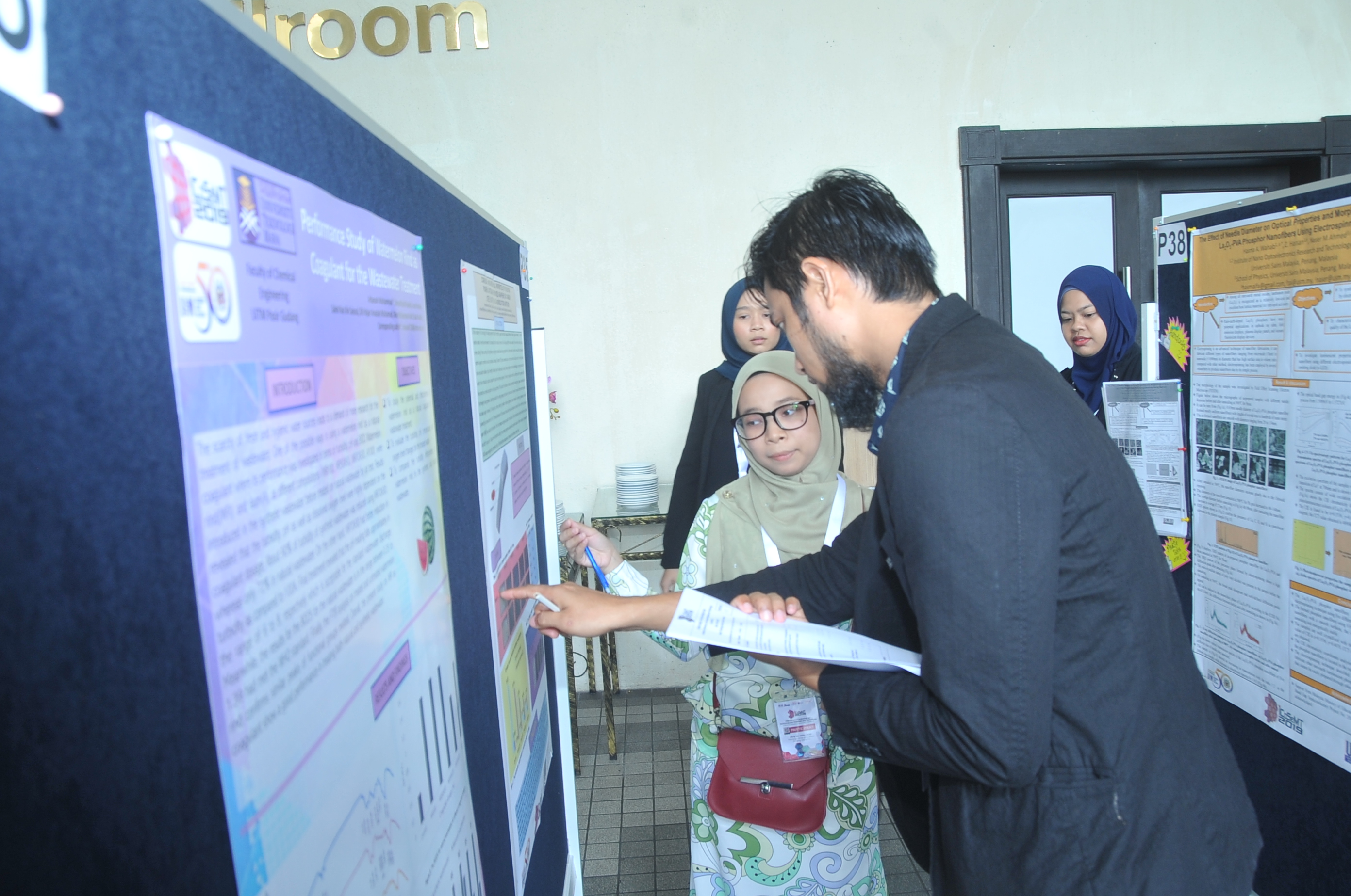
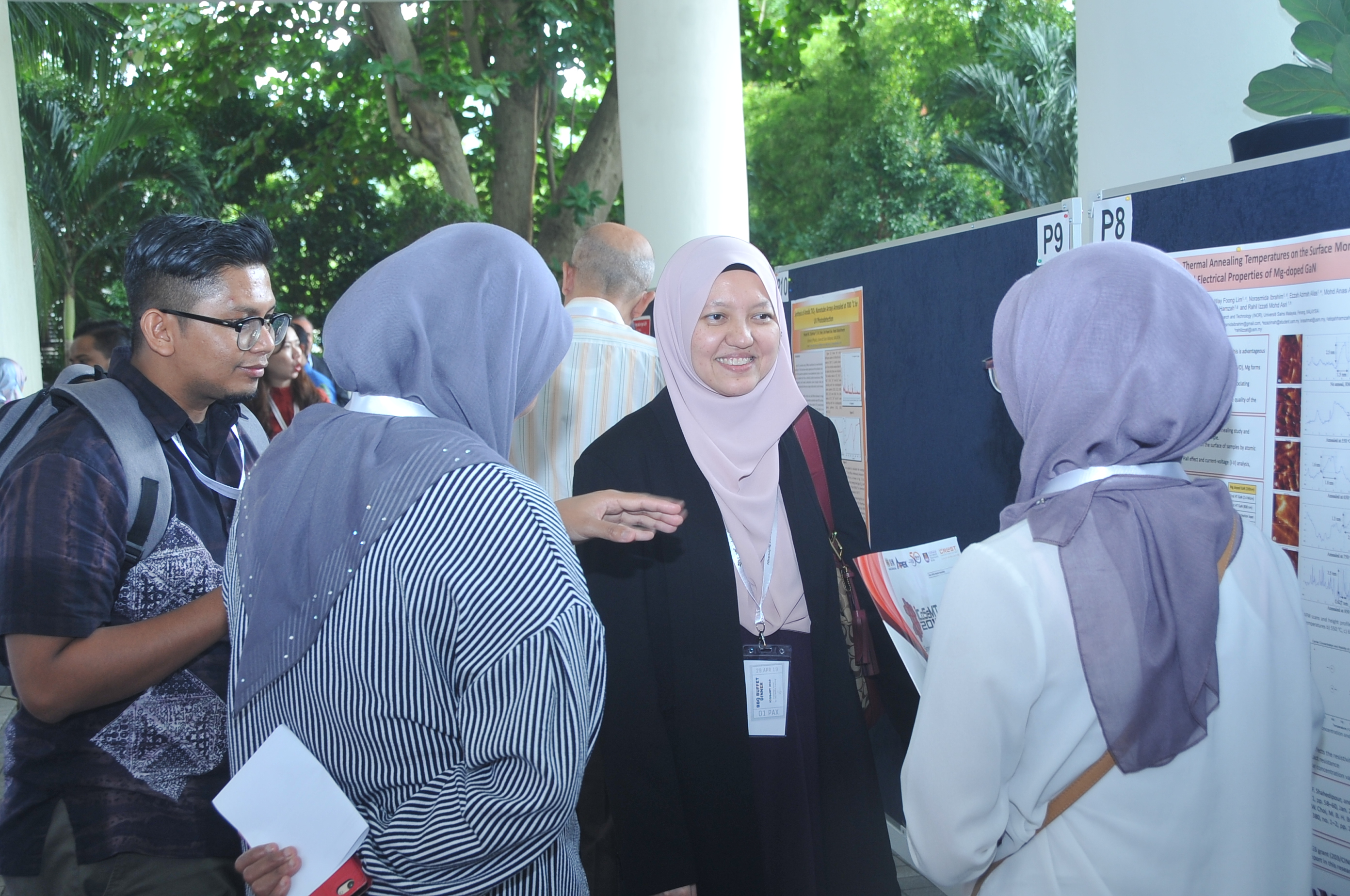
Your poster will be displayed during the Poster Session. There will be no Q&A session for poster presenters, however, the audience may submit their questions to your email during or after the conference.
TOPICS COVERED...
OPTICAL AND ELECTRONIC MATERIAL
| • | Narrow and Wide Band Gap Semiconductors |
|---|---|
| • | Diamond, Graphene and Carbon Nanotubes |
| • | Piezoelectric and Ferroelectric Materials |
| • | Electroluminescent Materials |
| • | Colour-Changing Materials |
| • | Energy Storage Materials |
| • | Dielectric Materials |
| • | Porous Structures |
| • | Nanostructures |
| • | Superconductors |
| • | Dielectric Materials |
| • | Porous Structures |
| • | Nanostructures |
| • | Superconductors |
ORGANIC AND POLYMERIC MATERIALS
| • | Organic Semiconductors |
|---|---|
| • | Conductive Polymers |
| • | Polymer Electronics and Coatings |
| • | Polymer Catalysts and Characterization |
| • | Composite Polymers and Biopolymers |
| • | Functional Polymers and Polymer Hybrid Materials |
DEVICES
| • | Optoelectronics |
|---|---|
| • | Sensors and Actuators |
| • | Power Devices |
| • | Novel Devices |
| • | Photovoltaics |
| • | MEMS/NEMS |
| • | Contacts and Interconnects |
| • | Fabrication Processes |
| • | Integrated System Design |
| • | Modelling and Simulation |
| • | MEMS/NEMS |
| • | Contacts and Interconnects |
| • | Fabrication Processes |
| • | Integrated System Design |
| • | Modelling and Simulation |
PACKAGING TECHNOLOGY
| • | Phosphor Technology |
|---|---|
| • | Lens and Optics |
| • | Thermal Management |
| • | Front End Assembly Processes |
| • | Back End Processes and Applications |
| • | Failure Analysis and Reliability |
IMPORTANT DATES
| Abstract Submission Deadline (Early Bird) | 15 September 2021 |
|---|---|
| Abstract Submission Deadline (Normal) | 8 October 2021 |
| Notification of Acceptance/Rejection | 1 Week after abstract submission |
| Payment Deadline | 24 October 2021 |
| Video Submission Deadline | 24 October 2021 |
| Full Paper Submission Deadline | 30 November 2021 |
SPEAKERS
Keynote Speaker
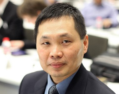
Institute of Nano Optoelectronics Research and Technology (INOR), USM, Malaysia
Visible light communication (VLC or LiFi) has been a topic of intense research after the idea was proposed in 2011. To date, a data rate of multiple 100s Mbps has been demonstrated using LEDs or micro-LEDs as transmitters. At KAUST, we are developing laser-based device and system technologies for Gbps VLC and underwater wireless optical communication (UWOC). In this talk, I will give a brief overview on recent deployments of Gbps VLC and UWOC systems. I will focus my discussion on recent developments of high-speed lasers, and self-powered and omnidirectional receivers for VLC and UWOC.
Boon S. Ooi is a Professor of Electrical and Computer Engineering at KAUST (Saudi Arabia), and an Adjunct Professor of the University of Science, Malaysia. He received the Ph.D. degree in electronics and electrical engineering from the University of Glasgow (Scotland, UK). He has served as a faculty member at Nanyang Technological University (Singapore) and Lehigh University (Pennsylvania, USA). His research interest includes the study of III-V and III-Nitride based materials and devices, and their applications in optical sensors and optical communications. He is a Senior Editor of IEEE Photonics Journal and Associate Editor of OSA Optics Express. Ooi is an elected fellow of the U.S. National Academy of Inventors (NAI). He is a Fellow of OSA, SPIE and IoP (UK).

United Kingdom
A microdisplay has a wide range of applications in smartphones, smartwatches, AR/VR systems, Helmet Mounted Displays (HMD), Head-Up Displays (HUD). Their individual pixel elements typically consist of a large number of micro-LEDs (μLEDs). Current μLEDs are far from satisfactory, as a number of fundamental challenges cannot be met by any existing technologies. Visible light communication (VLC) is an emerging technology that offers approximately 300 THz of license-free bandwidth that is four orders of magnitude larger than that available in current RF-based Wi-Fi or 5G. Unfortunately, the current approaches to the fabrication of VLC are substantially limited to μLED fabrication technologies. The conventional approach to the fabrication of μLEDs requires a combination of a standard photolithography technique and subsequent dry-etching processes. This approach unavoidably introduces damage during the dry-etching and following processing, severely degrading the optical performance of μLEDs. This issue becomes increasingly severe as the μLED dimensions decrease. The Sheffield team has developed a direct epitaxial approach to the fabrication of ultra-small and ultra-compact μLEDs for microdisplay application, leading to the 1st demonstration of ultra-small green μLEDs (3.6 μm diameter) without using dry etching (ACS Photonics 7, 411 (2020)), where our μLEDs exhibit a record EQE of 9% and the narrowest spectral linewidth (ACS Nano 14, 6906, (2020)). Our epitaxial integration has also led to the demonstration of a record modulation bandwidth of 1.2 GHz for VLC application (ACS Appl. Electron. Mater. 3, 445 (2021)) and 1st monolithically integrated μLEDs/HEMTs microdisplay on a single chip (Adv. Mater. Technol. 9, 2100214(2021)).
Tao Wang is a Professor (with Top Professor Grade) as Chair in Advanced Opto-Electronics in the Department of Electronic and Electrical Engineering, the University of Sheffield, the UK. He is Director of the Sheffield Centre for GaN Materials and Devices. He received his Ph.D. from Universität Würzburg in Germany in 1997. He started III-nitrides research at the University of Tokushima in Japan in 1997 and then worked at Nitride Semiconductor Ltd. in Tokushima as the R & D director from 2000 to 2002. He joined the University of Sheffield in August 2002 to carry on III-nitrides research. He was awarded the highly prestigious “EPSRC Advanced Research Fellow” in the UK in 2005. The innovation of his research led to two spinouts (Seren Photonics Ltd., the recipient of the 2015 Royal Society Emerging Technology Award; EpiPix Ltd. aiming to manufacture micro-LEDs). He is regularly involved in organizing international conferences including being Chair of the 16th International Symposium on the Science and Technology of Lighting in 2018 and the Chair of the 2012 Summer School on III-nitrides. He initiated and chaired the 1st China-UK workshop on GaN Materials and Devices. He has > 500 publications including 5 book chapters, > 250 journal papers, >250 conference papers and presentations. He holds 22 patents on III-nitrides.

Component level packaging is needed to protect integrated circuits from mechanical damage and to provide convenient electrical contacts for incorporating the circuits into larger systems. The choice of a type of package typically involves a trade-off between performance, reliability, and costs. A wide variety of materials: plastics, metals, ceramics, composites, etc., are used in packaging and there are many packaging technologies in use. For a better understanding of how packages degrade and eventually fail, models are being developed to describe their behavior. Calculating the thermal and mechanical properties of packages can be challenging because the dimensions of the smallest features inside a package can be much smaller than the size of the package thus requiring a fine spatial grid. The relevant time scales can range from nanoseconds for electronic signals to weeks for the diffusion of water in a package. These disparate and length scales often require that approximations be made. Some recent research on microelectronics packaging will be discussed.
Peter Hadley is a device physicist who has investigated superconducting circuits, single-electron circuits, carbon nanotube and single-molecule devices, organic semiconducting devices and inorganic semiconducting devices made from Si, and SiC. The current focus of his research is on understanding defects in semiconductors. He is the director of the Institute of Solid State Physics at the Graz University of Technology.
Plenary Speaker
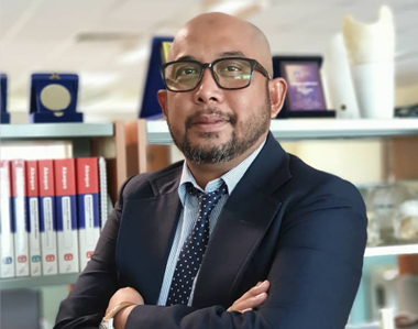
The growth of GDP for any country relies on the ability to produce goods i.e. commodities or manufacturing. In the last 10 years, although growing, the rate of the manufacturing sector in the country is slowing down and almost reaching its maintenance level. This can relate directly to the shift of demand from Western World consumers to cheaper affordable products from China and more recent competitors like Vietnam and Indonesia. Without manufacturing, the Malaysian E&E sector will continue to be diluted within the global supply chain. Therefore, how can we stay strong together riding this journey?
M SHAHRUL AZMI M YUSOFF, PhD
M Shahrul Azmi M Yusoff is currently the Director of Innovation in Smart Manufacturing at Standard and Research Institution of Malaysia (SIRIM). His PhD was in the study of acoustic detection and signal processing for predictive maintenance.
With over 18 years of experience in the industry, his publications include journals and technology articles. He is currently pursuing advanced research in predictive maintenance using artificial intelligence technology as part of the implementation strategy within the I4.0 Centre of Excellence.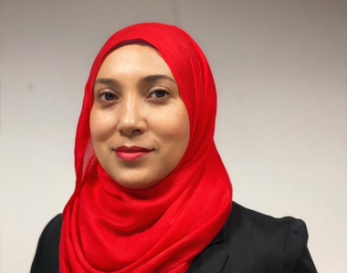
Ministry of Science, Technology and Innovation (MOSTI), Malaysia
Nanotechnology is making a revolution in manufacturing and production, creating new materials and products through novel processes for commercial purposes. New products based on nanotechnology with novel characteristics are continued to grow and benefit society like nanomaterials, particularly carbon nanotubes or graphene could offer semiconductors. Technology development towards experimental development research is moving forward on producing new products or improving existing products or processes. A newly developed method to reduce the size of semiconductor materials, dramatic improvements in the chemical, physical and structure properties of these materials continue to arise. Thus, minimizing the size in nanometer-scale of semiconductor materials has been shown to maximize the performance of semiconductors for their application in a wide range of material applications such as in energy sector, electronic device systems, automotive and etc.
Ruslinda binti A. Rahim received the Doctor of Philosophy (Ph.D) majoring in Nanoscience and Nanoengineering from Waseda University, Japan in September 2012. She also received M. Eng and B. Eng degree in Electrical and Electronic Engineering from Muroran Institute of Technology, Japan in 2007 and 2002, respectively. Currently, she is a Director of National Nanotechnology Centre under Ministry of Science, Technology and Innovation (MOSTI). She also a Research Fellow in Institute of Nano Electronic Engineering (INEE), Universiti Malaysia Perlis (UniMAP) and Associate Research Fellow in Institute of Microengineering and Nanoelectronics (IMEN), The National University of Malaysia (UKM). Her research interests include Nanoelectronics, Nanostructure device, Biosensors, Bioelectronics, DNA and protein detection, Aptamer and surface chemistry on carbon-based materials. She also active in several societies such as a Board of Engineers Malaysia, Professional Technologist Malaysia (MBOT) (Nanotechnology), Committee member of Malaysia Nanotechnology Association, Board of Member Malaysia Sensor Society and Editor of the International Journal of Nanoelectronics and Materials.
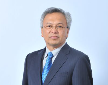
In the business world, this is the world of the fittest to survive. To this, businesses around the world always seek for improvement to stay competitive as demand from the customers particularly in the terms of price reduction. We can see the price of a computer in Malaysia. In the mid-80s, a white box PC was sold at RM 5000 at least. There was no laptop or notebook at that time. Tablet is far from available. Now a fairly good PC can be obtained at less than half this price.
In this session, it will be a sharing looking at both the hard and the soft management tools in manufacturing to stay competitive. Those who are able to exploit and constantly drive for changes that lead to improvement, innovation and breakthrough will always be in the game. Those who are not able to be in this game will eventually be out of business or being acquired by others. Some of these companies are history and some had created history.
DATO’ DR MOHD SOFI OSMAN
Dato’ Dr Mohd Sofi Osman was born in Penang. Received his primary and secondary educations in Penang before pursuing his engineering degree at the University of Strathclyde, Glasgow. He is married with three children.
Dato’ Dr Mohd Sofi Osman joined Intel in 2015 with the acquisition of Altera Corporation, where he was the Vice President and Managing Director and led Worldwide Operations and Engineering for the Asia Pacific region since 2012. Before joining Altera, he had a 25-year career at Advanced Micro Devices (AMD), culminating in his role as Corporate Vice President and Managing Director of AMD Penang. He holds a patent in the field of the semiconductor manufacturing process and has published papers on continuous improvement projects in backend semiconductor manufacturing. He retired from Intel in July 2016 after spending almost 30 years in the Semiconductor Industry. In 2018, he came out from retirement to work for Lumileds as Vice President and Managing Director of Lumileds Malaysia until June 2020.
Dato’ Dr Mohd Sofi Osman was on the Board of Directors at University Malaysia Perlis (UniMAP) since the organization was still known as KUKUM. He was the past Chairman of the board for University Malaysia Perlis and University Tun Hussein Onn Malaysia. He was also the Adjunct Professor at University Technology Mara (UiTM) Shah Alam and University Science Malaysia (USM).
He was the past Chairman of Penang Skills Development Centre (PSDC). He was also the past President of the Free Industrial Zone Penang Company Association (Frepenca).
He is currently the Advisor to Collaborative Research in Engineering, Science & Technology (CREST) Board, member of the CEO Faculty Program. He is currently an Adjunct Professor at the Institute of Nano Optoelectronics Research and Technology (INOR), University Science Malaysia with the mission of accelerating the research collaboration between INOR and industry players as well as assisting the advancement of research capabilities at INOR that are in line with industry’s needs.
Invited Speaker
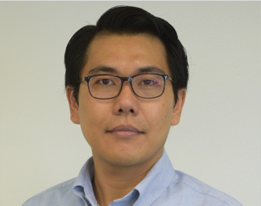


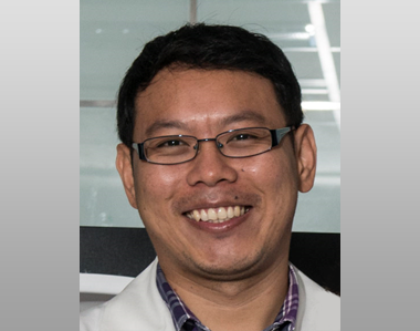

Hurry up! Grab this opportunity to submit your abstract.
Call for Paper
All abstracts will be peer-reviewed prior to the acceptance and identified either for oral or poster presentation.
All accepted abstracts will be invited to submit their full papers to be published in either Institute of Physics (IOP) Journal of Physics: Conference Series (JPCS)(Scopus-Indexed Proceeding), Solid State Phenomena (Scopus-Indexed Journal) (Publication fees: RM 500/USD 150) or other ISI-indexed journals.Conference Fee
- for Local participant
- • LIVE Online Keynote speech, Plenary speech,
and Scientific sessions - • Virtual Exhibition and Poster session
- • Program e-Book
- • e-Certificate of participation
- for Local participant
- • LIVE Online Keynote speech, Plenary speech,
and Scientific sessions - • Virtual Exhibition and Poster session
- • Program e-Book
- • e-Certificate of participation
- for Local participant
- • LIVE Online Keynote speech, Plenary speech,
and Scientific sessions - • Virtual Exhibition and Poster session
- • Program e-Book
- • e-Certificate of participation
- for International
- • LIVE Online Keynote speech, Plenary speech,
and Scientific sessions - • Virtual Exhibition and Poster session
- • Program e-Book
- • e-Certificate of participation
- for International
- • LIVE Online Keynote speech, Plenary speech,
and Scientific sessions - • Virtual Exhibition and Poster session
- • Program e-Book
- • e-Certificate of participation
RM 1000
- • HALF/FULL page advertisement.
- • Logo/Banner in ICoSeMT's official website.
- • Short advertisement video during break.
- • Virtual Exhibition slot (only for RM 1,000 package).
| • | Phosphor Technology |
|---|---|
| • | Lens and Optics |
| • | Thermal Management |
| • | Front End Assembly Processes |
| • | Back End Processes and Applications |
| • | Failure Analysis and Reliability |
All submitted papers will go through the peer-review process, we would also like to invite reviewers to help uphold the quality of submissions. An “Electronic Certificate of Appreciation” will be provided to all reviewers. If you are interested, please register HERE!
Payment Method
Payment Methods *
Cheque, L.O. / P.O., Electronic Fund Transfer, Cash Deposit
Instruction
You can pay your registration/publication fee using any of the following methods.
i) Cheque (Company Cheque only) / Bank Draft / Money Order / L.O. / P.O. must be made payable to “USAINS HOLDING SDN. BHD.”
ii) Automated Teller Machine (ATM) & Cash Deposit, Over-the-counter (OTC)
iii) Online Banking (Electronic Fund Transfer - EFT, Telegraphic Transfer - TT)
Please upload the payment proof (PO, Bank-in Slip, etc.) through your ICoSeMT user account. Please use your name as the file name.
Payee Details
a) Payee Name & Address:
USAINS HOLDING SDN. BHD., Level 2, Block C, SAINS@usm, No. 10 Persiaran Bukit Jambul, 11900 Bayan Lepas, Penang.
b) Bank Transfer Details:
Account Name: USAINS HOLDING SDN. BHD.
Name of Bank: AmBank (M) Berhad, Level 21, Menara Dion, Jalan Sultan Ismail, 50250 Kuala Lumpur.
Account Number: 888 – 100 – 985 - 0380
Swift Code: ARBKMYKL
c) Details:
2nd International Conference on Semiconductor Materials and Technology (ICoSeMT 2021) and International Innovation, Invention & Design Expo (INoDEx 2021)
Remark
Payment should be 'NO' later than October 24th, 2021. No refund policy will be adopted in this event.
Exhibitor Package
PACKAGE A
HALF page advertisement in program book.
Logo/Banner in ICoSeMT's official website.
Short advertisement video (2.00 minutes duration) will be played when audiences click on the respective company logo in ICoSeMT's official website.
PACKAGE B
Logo/Banner in ICoSeMT's official website.
Short advertisement video (2.00 minutes duration) will be played when audiences click on the respective company logo in ICoSeMT's official website.
Virtual Exhibition on ICoSeMT's official website.
Our Sponsors
Check Who Makes This Event Possible!
Business Events Sarawak
Nexus Analytics Sdn Bhd
Inno Lab Engineering Sdn Bhd
Opportunities
Learn & Share
Ask Expert
Explore Event
Publish Your Article
Take a look at our 1st ICoSeMT 2019!
