
ABOUT ICoSeMT
3rd International Conference on Semiconductor Materials and Technology (3rd ICoSeMT 2023) is a biennial event that is jointly organized by Institute of Nano Optoelectronics Research and Technology (INOR), Universiti Sains Malaysia (USM), Universiti Teknologi MARA Cawangan Pulau Pinang (UiTMCPP), National Nanotechnology Centre (NNC), Ministry of Science, Technology and Innovation of Malaysia (MOSTI), MIMOS Berhad and Collaborative Research in Engineering, Science & Technology (CREST) with the Theme “Innovation Towards A Sustainable Tomorrow”. The primary focus of the conference is to create an effective medium for institutions and industries to share ideas, knowledge, and expertise in the fields related to Semiconductor Materials and Technology.
This year, with the aim to promote positive innovation culture and encourage innovation activities and from different walks of life, a sub-event entitled International Invention, Innovation & Design Expo (INoDEx 2023) is going to be held concurrently. This sub-event will be a great platform in creating opportunities for local and international participants to present their innovations and inventions. Eventually, both events will lead to interaction and future collaboration among the local and international participants.
TOPICS COVERED...
OPTICAL AND ELECTRONIC MATERIAL
- Narrow and Wide Band Gap Semiconductors
- Diamond, Graphene and Carbon Nanotubes
- Piezoelectric and Ferroelectric Materials
- Electroluminescent Materials
- Colour-Changing Materials
- Energy Storage Materials
- Dielectric Materials
- Porous Structures
- Nanostructures
- Superconductors
ORGANIC AND POLYMERIC MATERIALS
- Organic Semiconductors
- Conductive Polymers
- Polymer Electronics and Coatings
- Polymer Catalysts and Characterization
- Composite Polymers and Biopolymers
- Functional Polymers and Polymer Hybrid Materials
DEVICES
- Optoelectronics
- Sensors and Actuators
- Power Devices
- Novel Devices
- Photovoltaics
- MEMS/NEMS
- Contacts and Interconnects
- Fabrication Processes
- Integrated System Design
- Modelling and Simulation
PACKAGING TECHNOLOGY
- Phosphor Technology
- Lens and Optics
- Thermal Management
- Front End Assembly Processes
- Back End Processes and Applications
- Failure Analysis and Reliability
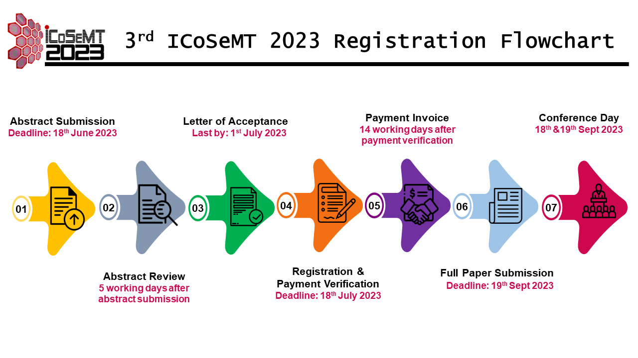
IMPORTANT DATES
| Abstract Deadline | 1 May 2025 | ||
|---|---|---|---|
| Notification of Acceptance | 18 June 2025 | ||
| Registration and Full Paper Submission Deadline | 18 July 2025 | ||
| Payment Deadline | 18 July 2025 | ||
| Conference Date | 29 & 30 Sept 2025 |
Keynote Speaker
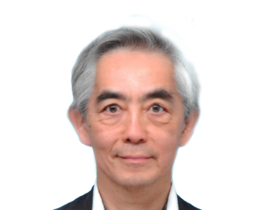
PROF. DR. HIROSHI KAWARADA
Waseda University
Japan
Semiconductor circuits are typically constructed of both n-channel FETs (n-FETs) and p-channel FETs (p-FETs), whose dual polarity capabilities provide advantages in switching speed and energy efficiency. However, in high voltage circuits such as inverters and converters, both the upper and lower arms are composed of n-FETs. The circuit is not symmetrical and requires additional components to work properly, but at the cost of lower efficiency and switching speed. Here, we propose a complementary circuit based on symmetrical operation by adding a power p-FET with performance equivalent to a power n-FET. There are no power p-FETs other than Diamond. Diamond p-FETs now approach or exceed the characteristics of SiC or GaN n-FETs. While single-crystalline diamonds are still 1 to 2 inches in diameter, polycrystalline diamonds are larger than 4 inches and can be used in power and high-frequency FETs. Grain boundaries are not leakage paths for hole conduction in p-FETs. We are close to realizing complementary high-voltage circuits that have never existed in electronics.
Prof. Dr. Hiroshi Kawarada received Doctor of Engineering from Waseda University (1985) and joined Osaka University as Assistant Professor at Osaka, University (1986) where he started diamond research. Later, he worked in Waseda University as Associate Professor (1990) and Professor (1995-), where he developed C-H diamond FET in 1994. As Visiting Researcher he stayed in Fraunhofer Institute (IAF) by Fellowship of Alexander von Humboldt Foundation (1995-1996). As an organizer he served for European Conference on Diamond and Related Materials (1998-2008). In Japan, he also served for Japan Applied Physics Society as Board Member, New Diamond Forum as Chairman (2009-2014) and Science Council of Japan as Member. His research field is nanoelectronics, bioelectronics and power electronics using diamond, where he has 380 articles with about 10000 citations.
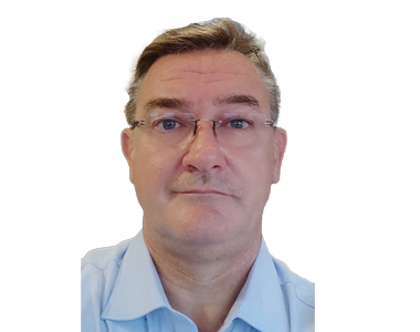
DR. DAVID LACEY
ams OSRAM
Malaysia
The talk will discuss application trends in the optoelectronics industry and the underlying technical challenges that must be addressed to serve those markets. Applications of monolithic multi-pixel devices, discrete microLED devices and laser devices will be explored and recent progress & future challenges discussed.
Dr David Lacey is Director of Advanced Development & Services, R&D for Osram Opto Semiconductors (M) Sdn Bhd, Penang – part of the ams OSRAM group. He has been based in Malaysia for more than 20 years and is currently a Board Member of Collaborative Research in Engineering, Science & Technology (CREST) and the President of FREPENCA – the Free Industrial Zone, Penang Companies Association. He also represents ams Osram at SFAM – The Semiconductor Fabrication Association of Malaysia since the association’s foundation in 2016.

TS. DR. LEE HING WAH
MIMOS Berhad
Malaysia
ABSTRACT:-
The Malaysian Electronics and Electrical (E&E) industry has stood as a pillar of the nation's economy for the past five decades, consistently ranking as the country's top exporter. Traditionally, Malaysia has excelled in the semiconductor value chain, particularly in the back-end activites, with ATP (Assembly, Testing, and Packaging) operations, boasting a significant 13% share of the global market in this domain. However, despite these achievements, the industry's overall contribution to the nation's GDP remains relatively modest, hovering around 6.9%.
Recognising the imperative for our local E&E sector to ascend to the higher value chain, it is essential to bolster its role in driving higher GDP growth for the nation. This endeavor aligns seamlessly with the objectives outlined in the recently launched New Industrial Master Plan (NIMP 2030) and the E&E Roadmap: Technology Development 2021-2030.
In this keynote presentation, our speaker will delve into a comprehensive analysis of the global and local E&E Semiconductor industry. More importantly, they will explore strategies to propel our nation up the E&E value chain though high-value semiconductor technology (HVST), harmonising with national policies and leveraging the pivotal role of strategic agencies such as MIMOS in order to collectively work towards realising our national aspirations and fostering sustainable economic growth.
Keywords: Semiconductor, E&E, high-value semiconductor technology, HVST, NIMP 2030, MIMOS
- Head of Semiconductor-areas of research and is responsible for the development of Semiconductor technology, Nanotechnology-based materials, process technologies and sensors/devices to support the Semiconductor and E&E Industry in Malaysia.
- Graduated with a PhD in Mechanical Engineering (MEMS) from University of Science Malaysia (USM) and has more than 17 years of industrial experience as a researcher.
- Ownership of >50 publications and filed patents in Nano/Semiconductor/Electronics and its related areas.
- Areas of research include:
- Semiconductor technologies such as Advanced Packaging, WBGSs, other niche areas such as AI, memristor,
- Nanomaterials and 2D-NM synthesis and characterization (ferromagnetic nanoparticles, metal oxide nanowires, carbon nanotubes, graphene and their derivatives).
- Incorporation of nanomaterials on MEMS and NEMS device platforms for sensors and electronics applications.
- Printed, flexible and wearable electronics.
- Chairman of the national mirror committee NSC 19/TC 12 (IEC TC113) on Nanotechnology for electrotechnical products and systems.
- Technical committee for NSC 19/TC 14 (IEC TC124) Wearable electronic devices and technology.
-
National Project Committee on Nanomaterials and National Technical Committee on Wearable Electronic Devices and Technologies.
Plenary Speaker
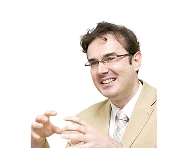
ASSOC. PROF. JEAN JACQUES DELAUNAY
University of Tokyo
Japan
This talk will review some of the recent trends in functional optical structures and particularly focus on the aspects of increased light-matter interaction via the design of optical micro-nano structures and integration of the micro-nano structures on a chip. Structures sustaining surface waves are first reviewed with a particular emphasis on their propagation lengths and ability to support on-chip integrated functional devices. Semiconductor microcavities supporting strong interaction between excitons and photons and leading to the formation of exciton-polaritons that can be applied in interferometric microdevices are then presented. Structures supporting bound states in the continuum with applications in lasing are also introduced. Finally, the enhancement of chiral signal in a cavity using 2D chiroptical material property is presented.
DR. JEAN- JACQUES DELAUNAY
Dr. Jean-Jacques Delaunay is an Associate Professor at the School of Engineering, The University of Tokyo. He received his Ph.D. degree from Strasbourg University. He has worked for research institutions in the fields of optics, photonics, and optical functional materials in France, Germany, and Japan. He conducts research on the synthesis of micro/nanomaterials with controlled structures and functionalities for sensing and energy conversion. He also conceives plasmonic nanostructures to enhance the sensitivity of detectors and improve the efficiency of light collection for solar energy conversion devices. His current research projects include the development of surface wave platforms for optical sensing and light-emitting devices. He has co-authored more than 100 scientific publications and serves as an APEX/JJAP editor.
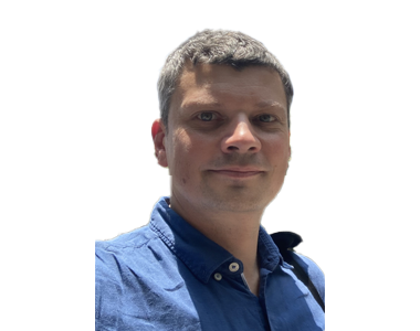
DR. GUENTHER MAIER
AT&S: Advanced Technologies & Solutions
Malaysia
ABSTRACT:-
IC Substrates are one of the key elements of advanced packaging and provide translation from the nano world of IC`s to the micro world of printed circuit boards. There they serve aspects including data transport, reliable electrical supply, thermal management and mechanical stability. Most of the advanced packaging concepts are built on the IC Substrate technology, including so-called chip first panel level packages and fan out packages.
I will introduce AT&S and the main concepts for substrate based advanced packaging technologies. In the second part, focuses on packages and modules highlight actual developments. Third, the materials and the support of advanced simulation technologies for the development of reliable packages will be targeted. The presentation with be closed with a summary.
Keywords: IC Substrates, Packaging, Materials, Virtual development
DR. GUENTHER MAIER
Dr. Guenther Maier Master in Chemistry (University of Graz, Austria), PhD in Materials Science (University of Leoben, Austria). 20+ years work experience as scientist (50+ papers in web of science), program manager and head of department at Materials Center Leoben Forschung. Since three years at AT&S, world-wide responsible for the research and university network development. Since more than 18 months engaged in Malaysia to build a sustainable network in research and higher education for IC Substrates and Advanced Packaging.
Invited Speaker
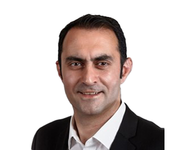
DR. YILMAZ DIKME
Element 3-5 GmbH
Germany
The epitaxial growth of compound-semiconductor thin films by metal-organic chemical vapor deposition (MOCVD) is counted as standard and mature technology. In this work growth results of thin aluminum nitride (AlN) and gallium nitride (GaN) layers grown by Next Level Epitaxy (NLE) process on sapphire, silicon and glass are presented. The growth temperature of the NLE layers are below 250°C surface temperature. The NLE process is a combination of PVD (physical vapor deposition) and CVD (chemical vapor deposition) and is following in principle the MOCVD growth standard. All steps use different plasma sources in various combinations including one DC- (direct current) bias and one RF (radio frequency)-bias. In total four different plasma sources have been used. As Al-source 99.999% pure Al was used. As nitrogen source nitrogen gas with a purity of 99.9995% was used which is introduced by a homemade ion gun. Additionally, argon, oxygen and hydrogen were used. The used plasma sources are all designed as stripe sources. First the substrates were cleaned with a mixture of argon and oxygen and after with argon and hydrogen using the RF-bias. After the in-situ cleaning first aluminum in monolayer range was deposited followed by low plasma power and low growth rate AlN and after higher plasma power and higher growth rate AlN. During the AlN growth additionally a DC-bias was used. The NLE AlN on sapphire was overgrown by MOCVD. The growth results of the various AlN and GaN thin films and their overgrowth in MOCVD will be presented.
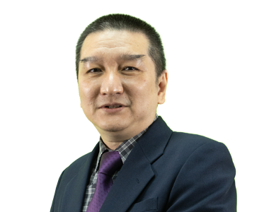
ASSOC. PROF. DR. NG SHA SHIONG
Universiti Sains Malaysia
Malaysia

DR. AZHARUL ARIF KAMARULZAMAN
ams OSRAM
Malaysia
Abstract
This slot aims to introduce the presence of epitaxy development department in ams-OSRAM located in Kulim, Kedah. The talk will begin with introducing an Intelligent Forward Lighting and Projection system that is capable of eliminating the risk of dazzling oncoming traffic and projecting warning symbols on the road for communication purposes. Aside from the advanced optics and drivers that made such lighting possible, the beating heart of this system is the light emitting diode (LEDs) layers that is grown by epitaxy. This talk will focus high volume production challenges when increasing the wafer diameter, and this is followed by potential solutions that can alleviate such issues.
Dr. Azharul Arif Kamarulzaman is a Staff Epitaxy R&D Engineer for Osram Opto Semiconductors (M) Sdn Bhd, Kulim – part of the ams OSRAM group, where he is currently working on new epitaxy product introduction. He has 5 years of experience with a balanced mixture of III-nitride epitaxy development, introduction and process sustaining. In 2023, he is selected as one of epitaxy key expert in high volume production within ams OSRAM. Along with this, he accumulates 11 years of experience in III-Nitrides materials growth and characteristics during his PhD studies with Institute of Nano Optoelectronics Research and Technology (INOR), USM

DR. SAI CHEONG LEE
ams OSRAM
Malaysia
Abstract
Optical product development is complex, expensive, risky and time consuming. A standard product development lifecycle covers ideation, demand validation, prototype, optimization, followed by manufacturing and commercialization. In practice, experimental design and assessment of product quality require long period of time and high resource consumption. To reduce complexity in experimentation, multiphysics simulations together with appropriate optimization techniques are usually carried out to find optimal design and materials until the product reaches satisfaction between performance, quality, manufacturability and cost. This presentation aims to highlight the role of physical modelling and optimization in optical product development. A few practical examples will be presented at a glance. First example is about the use of electro-optical modelling and a famous paradigm of swarm intelligence, namely, particle swarm optimization (PSO), to simplify the performance evaluation of different LED chip layout designs. The workability of PSO to solve design-optics problem was justified by the good agreement between experiment and simulation-proposed solution. Followed by the success of PSO, another example is given to the assessment of an improved version of PSO, namely, multi-objective PSO (MOPSO). Finally, examples are given to the optical modelling of LED packages for failure analysis and materials quality control.
Dr. Sai Cheong Lee is a computational physicist graduated from Universiti Sains Malaysia, currently working as a Senior Staff Modelling and Simulation Engineer in ams-OSRAM. His fields of specialization are LED optics, phosphor materials, applied optimization and simulation software development. With his effort in strengthening the cross-functional modelling and simulation competency in ams-OSRAM, he has won the OSRAM Wizard of OS: Commendation Award in 2019, followed by the appointment of Key Expert Modelling in 2021. Apart from the lighting technology, Dr. Lee has extensive experience on how physical modelling applied with infrared spectroscopy to characterize semiconductor materials. Despite his full-time engineer job, he is a volunteer scientist to provide complementary supervision for university postgraduate student and conduct peer review services for academic publisher such as Optica, IOP, Elsevier, etc. He was appointed by YSN-ASM (Young Scientist Network – Academy of Science Malaysia) as an industrial young scientist member since 2020.
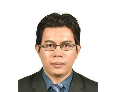
ASSOC. PROF. Ir. Ts. DR. MOHAMAD HAFIZ MAMAT
Universiti Teknologi MARA, Shah Alam
Malaysia
Abstract
In the past decade, humidity sensors have been the subject of extensive research and consideration in a wide variety of applications, including agriculture, food industries, climate monitoring, chemical storage, healthcare, and semiconductor industries, to name a few. The studies have been centred on the preparation of humidity sensors with good humidity sensing performance and low cost. These sensors are required to be manufactured on a large scale and must fulfil the stringent performance obligations of emerging areas. In this investigation, resistive-type humidity sensors made of zinc oxide (ZnO) nanomaterials were developed. The chemical solution immersion technique was utilised during the production of the ZnO nanomaterials. It is possible to produce nanostructured films on a large scale using this chemical solution immersion method, which is a fabrication process that is both cost-effective and efficient. The findings of this research indicate that ZnO nanomaterials could be promising candidates for use in applications involving humidity sensing. ZnO nanomaterials have a high sensitivity to humidity sensing, and they could provide potential applications for humidity sensing in emerging areas.
Assoc. Prof. Ir. Ts. Dr. Mohamad Hafiz Mamat graduated from the Department of Electrical and Electronic Engineering and Information Engineering at Nagoya University, Japan, in 2005 and received both an MSc degree and a PhD degree in Electrical Engineering from Universiti Teknologi MARA (UiTM) Shah Alam, Malaysia, in 2010 and 2013, respectively. Currently, he is the Coordinator of Publications for the College of Engineering and Head of the NANO-ElecTronic Centre (NET) at UiTM. His research area is in the field of nanoelectronics, which focuses on nanomaterial syntheses and the fabrication of electronic devices such as sensors, nanogenerators, and solar cells. He was awarded both Professional Engineer (Ir.) and Professional Technologist (Ts.) in 2018. He has published over 400 papers in journals and conference proceedings. He was assigned as a visiting scientist at BSA Rahman Crescent Institute of Science and Technology, Chennai, India, in 2018. He has received research grants of more than RM 2 million as a principal investigator and member from various agencies, such as the Ministry of Higher Education Malaysia and CREST. Up to now, he has 2 Malaysian patents and 32 copyrights registered at MyIPO. He joined several conferences and symposia at the international and national levels as a participant, invited speaker, and keynote speaker. He also serves as the head of the technical committee for NANO-SciTech conferences.
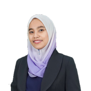
ASSOC. PROF. DR. NORZAINI ZAINAL
Universiti Sains Malaysia
Malaysia
Abstract
Aluminum gallium nitride based ultra-violet light emitting diodes (AlGaN based UV LEDs) have recently gained much attentions owing to their potential in various areas of applications, including virus disinfection and water purification. Nonetheless, commercially available UV LEDs today are only few percent efficient, making them are not energy- and cost-efficient for large-scale environments. Of the key approach to increase the LEDs efficiency is to grow the LEDs on low threading dislocation density (TDD) aluminum nitride (AlN) layer. An ideal route to obtain such AlN layer is by growing the layer on native AlN substrate. However, such substrate is currently expensive and available in limited sizes. To date, most of AlN layers are grown on sapphire substrate (AlN/sapphire templates), which commonly serve as pseudo-substrates for the UV LEDs. At this point, it is still a challenge to obtain AlN/sapphire templates with the TDD of lower than 109 cm-2 in the effort towards improving the UV LEDs efficiency.
This talk will present results from optimization works for the growth of AlN/sapphire templates at INOR, USM. In particular, the first part of this talk discusses on the effect of nitridation time, nitridation temperature, nucleation time on reducing the TDD in the AlN/sapphire template with the growth temperature, Tg above 1200 °C. With the optimum parameters, the TDD in the template can be as low as ~8.6 ×108 cm-2. Meanwhile, the surface is atomically smooth with improved steps-like structure. The second describes the role of trimethylaluminum (TMAl) preflow in maintaining the material quality of the AlN/sapphire templates when the templates were grown at a lower Tg , of which around 1175 °C. The last part proposes the potential of our AlN/sapphire in realizing workable UV LEDs.
Assoc. Prof. Dr. Norzaini Zainal is currently an Associate Professor at Universiti Sains Malaysia. At her early career, she spent almost two years working on cubic gallium nitride (GaN) material, which was an extended project from her PhD work at University of Nottingham, UK. Later, she initiated a new research theme in nitrides semiconductors, focusing on controlling properties of nitrides thin films through base structuring in nanoscale and base crystal orientation, together with manipulation of processing physically and thermally. In recent years, her team has worked extensively in improving material properties of Al(Ga)N and GaN as base layers for ultraviolet (UV) and visible light emitting diodes (LEDs) through epitaxial technology based metal organics chemical vapor deposition (MOCVD). They also focus on designing and developing LEDs operating in UV and green spectral regions. So far, Norzaini Zainal’s team has collaborated with several leading groups in nitrides; e.g. University of California, Santa Barbara, USA, Université Côte d¢Azur, France, King Abdullah University of Science and Technology (KAUST), and the latest, Ferdinand Braun Institute, Germany.
Mr. IRFAN ABD RAHMAN
Infineon Technologies Sdn. Bhd.
Malaysia
Hurry up! Grab this opportunity to submit your abstract.
Call for Paper
All full papers will be considered for publication in AIP Conference Proceedings
(Scopus-Indexed Proceeding)
Conference Fee
- for Local participant
- • Admission to keynote speech, plenary speech,
and scientific sessions - • Admission to exhibition
- • Certificate of participation
- • Coffee break, lunch and tea break for 2 days
- • Buffet dinner on the first day of conference
- for Local participant
- • Admission to keynote speech, plenary speech,
and scientific sessions - • Admission to exhibition
- • Certificate of participation
- • Coffee break, lunch and tea break for 2 days
- • Buffet dinner on the first day of conference
- for International
- • Admission to keynote speech, plenary speech,
and scientific sessions - • Admission to exhibition
- • Certificate of participation
- • Coffee break, lunch and tea break for 2 days
- • Buffet dinner on the first day of conference
Payment Method
Payment Methods *
Cheque, L.O. / P.O., Electronic Fund Transfer, Cash Deposit
Instruction
You can pay your registration/publication fee using any of the following methods.
i) Cheque (Company Cheque only) / Bank Draft / Money Order / L.O. / P.O. must be made payable to “USAINS HOLDING SDN. BHD.”
ii) Automated Teller Machine (ATM) & Cash Deposit, Over-the-counter (OTC)
iii) Online Banking (Electronic Fund Transfer - EFT, Telegraphic Transfer - TT)
Please upload the payment proof (PO, Bank-in Slip, etc.) through your ICoSeMT user account. Please use your name as the file name.
Payee Details
a) Payee Name & Address:
USAINS HOLDING SDN. BHD., Level 2, Block C, SAINS@usm, No. 10 Persiaran Bukit Jambul, 11900 Bayan Lepas, Penang.
b) Bank Transfer Details:
Account Name: USAINS HOLDING SDN. BHD.
Name of Bank: AmBank (M) Berhad, Level 21, Menara Dion, Jalan Sultan Ismail, 50250 Kuala Lumpur.
Account Number: 888 – 100 – 985 - 0380
Swift Code: ARBKMYKL
c) Details:
3rd International Conference on Semiconductor Materials and Technology (ICoSeMT 2023) and 2nd International Innovation, Invention & Design Expo (INoDEx 2023)
Remark
Payment should be 'NO' later than July 18th, 2023. No refund policy will be adopted in this event.
Booth Exhibition Packages
- 1) Booth space measurement = 5m (W) x 2m (D) x 2.5m (H) = 10sqm
- 2) List of items prepared by organizer:
- - Booth Panels (4 panels: 2 panels = 2m x 2.5m and 2 panels = 2.5m x 2.5m)
- - 1 unit info table / Banquet table (1m (L) x 0.5m (W) x 0.75m (H))
- - 1 set of company name stickers cut out
- - 2 units of flip chair
- - 1 unit dustbin
- - 2 units tube light
- - 1 unit 13 amp power point
- - 1 unit fan
- 3) 2 pax for 2 days (conference kits +access to all conf. Presentation + meals (excluded dinner)
- 4) Logo (with company link) at landing page of ICoSeMT's official website.
- 5) Short advertisement video (2 min duration) will be played when audiences click on the respective company logo on the landing page of ICoSeMT's official website.
- 6) Full page advertisement in Program book:
- - Full page of B5 Size
- - Dimension (Width x Height): (176 mm x 250 mm) in Portrait format.
- - Camera ready and full colour in pdf, jpeg, or png format
- Bank Information:
- Account Name : USAINS HOLDING SDN. BHD.
- Bank : AmBank (M) Berhad
- Account Number: 888 – 100 – 985 - 0380
- Swift Code: ARBKMYKL
- Should you have any enquiries, kindly contact us at the following information:
- Assoc. Prof. Dr. Ng Sha Shiong (shashiong@usm.my | 013-4729700)
- 1) Booth space measurement = 2.5m (W) x 2m (D) x 2.5m (H) = 5sqm
- 2) List of items prepared by organizer:
- - Booth Panels (3 panels: 2 panel = 2m x 2.5m and 1 panel = 2.5m x 2.5m)
- - 1 unit info table / Banquet table (1m (L) x 0.5m (W) x 0.75m (H))
- - 1 set of company name stickers cut out
- - 2 units of flip chair
- - 1 unit dustbin
- - 2 units tube light
- - 1 unit 13 amp power point
- - 1 unit fan
- 3) 2 pax for 2 days (conference kits +access to all conf. Presentation + meals (excluded dinner)
- 4) Logo (with company link) at landing page of ICoSeMT's official website.
- 5) Short advertisement video (2 min duration) will be played when audiences click on the respective company logo on the landing page of ICoSeMT's official website.
- 6) Full page advertisement in Program book:
- - Full page of B5 Size
- - Dimension (Width x Height): (176 mm x 250 mm) in Portrait format.
- - Camera ready and full colour in pdf, jpeg, or png format
- Bank Information:
- Account Name : USAINS HOLDING SDN. BHD.
- Bank : AmBank (M) Berhad
- Account Number: 888 – 100 – 985 - 0380
- Swift Code: ARBKMYKL
- Should you have any enquiries, kindly contact us at the following information:
- Assoc. Prof. Dr. Ng Sha Shiong (shashiong@usm.my | 013-4729700)
- 1) Banner Display (with own design) at ICoSeMT 2023 Event Site
- 2) Including printing and setting up the banner on the retractable banner stands = 2.5 ft (W) x 6 ft (H)
- 3) Logo (with company link) at landing page of ICoSeMT's official website.
- 4) Short advertisement video (2 min duration) will be played when audiences click on the respective company logo on the landing page of ICoSeMT's official website.
- 5) Full page advertisement in Program book:
- - Full page of B5 Size
- - Dimension (Width x Height): (176 mm x 250 mm) in Portrait format.
- - Camera ready and full colour in pdf, jpeg, or png format.
- Bank Information:
- Account Name : USAINS HOLDING SDN. BHD.
- Bank : AmBank (M) Berhad
- Account Number: 888 – 100 – 985 - 0380
- Swift Code: ARBKMYKL
- Should you have any enquiries, kindly contact us at the following information:
- Assoc. Prof. Dr. Ng Sha Shiong (shashiong@usm.my | 013-4729700)
- 1) Logo (with company link) at landing page of ICoSeMT's official website.
- 2) Short advertisement video (2 min duration) will be played when audiences click on the respective company logo on the landing page of ICoSeMT's official website.
- 3) Full page advertisement in Program book:
- - Full page of B5 Size
- - Dimension (Width x Height): (176 mm x 250 mm) in Portrait format.
- - Camera ready and full colour in pdf, jpeg, or png format.
- Bank Information:
- Account Name : USAINS HOLDING SDN. BHD.
- Bank : AmBank (M) Berhad
- Account Number: 888 – 100 – 985 - 0380
- Swift Code: ARBKMYKL
- Should you have any enquiries, kindly contact us at the following information:
- Assoc. Prof. Dr. Ng Sha Shiong (shashiong@usm.my | 013-4729700)
- 1 Dinner Table for 10 pax
- Dinner course = International Buffet Style
- For more information, kindly contact us at the following information:
- Assoc. Prof. Dr. Ng Sha Shiong (shashiong@usm.my | +6013-4729700)
- Ts. Dr. Mohd Syamsul Nasyriq Bin Samsol Baharin (Event Manager)
- (nasyriq@usm.my | +6013-4679767)
SPONSORSHIP PACKAGES
- Sponsor cash for ICoSeMT 2023 and INoDEx 2023.
- (Minimum amount of RM 5,000)
- *Benefits:
- a) Double Tax Exemption
- b) Company name features on the certificate of the special award.
- c) Full page advertisement in the Program/Proceeding book.
- d) Logo at landing page of ICoSeMT's official website.
- e) Short advertisement video (2 min duration) will be played when audiences click on the respective company logo on the landing page of ICoSeMT's official website.
- *ONLY entitled to industry/company funders.
- Sponsor cash for special award recipients.
- (Minimum amount RM1,500 and above)
- Benefits:
- a) Company name features on the certificate of the special award.
- b) Tax exemption.
- c) Full page advertisement in the Program/Proceeding book.
- d) Logo at landing page of ICoSeMT's official website.
- e) Short advertisement video (2 min duration) will be played when audiences click on the respective company logo on the landing page of ICoSeMT's official website.
- Sponsor medals for special award recipients.
- (Minimum amount of RM 500)
- Benefits:
- a) Company name features on the medal and certificate of the special award.
- b) Tax exemption.
- c) Full page advertisement in the Program/Proceeding book.
- d) Logo at landing ICoSeMT's official website.
- The design and purchase of the medal and certificate can be prepared by either the committee members or the company with consent from both parties.
- Sponsor merchandise or gift for special award recipients.
- (Minimum amount of RM 500)
- Benefits:
- a) Company name features on the certificate of the special award.
- b) Tax exemption.
- c) Full page advertisement in the Program/Proceeding book.
- d) Logo at landing ICoSeMT's official website.
For more information, kindly contact us at the following information:
Assoc. Prof. Dr. Ng Sha Shiong (shashiong@usm.my | +6013-4729700)
Dr. Siti Juliana Abu Bakar (sitijuliana@uitm.edu.my | +6019-4752209)
Sponsorship (Package S1):
Kindly contact us for the procedure and banking following
Sponsorship (Packages S2-S4):
Bank Information:
Account Name : Universiti Sains Malaysia
Bank : CIMB Bank Berhad
Account Number : 98986101402447
OUR SPONSORS VIDEO
Opportunities
Learn & Share
Ask Expert
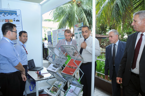
Explore Event
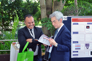
Publish Your Article
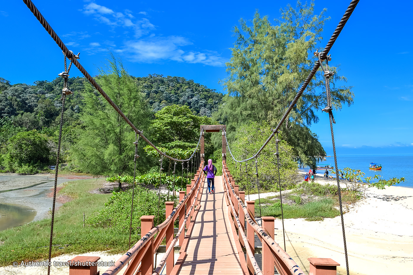
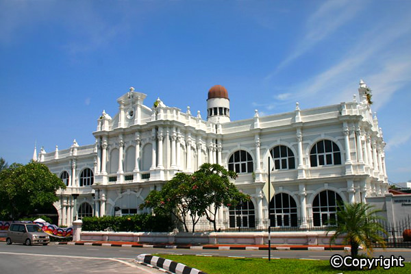
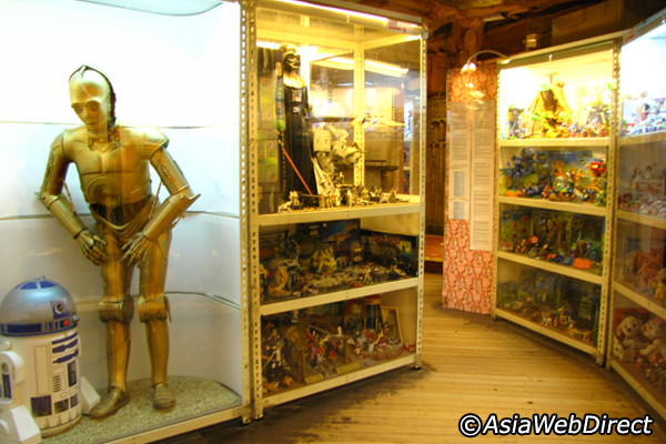
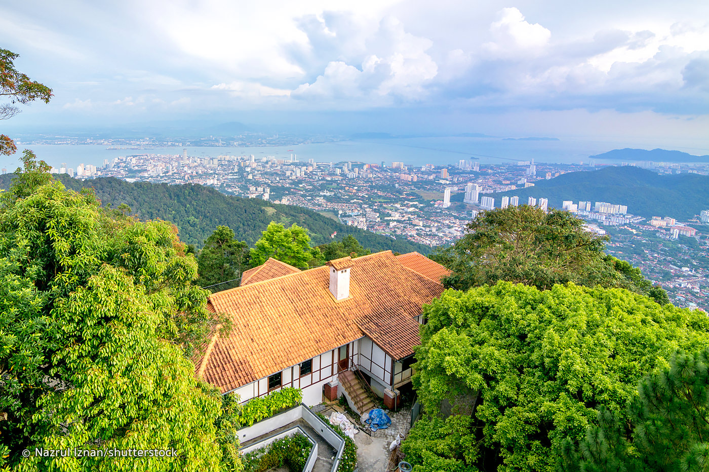
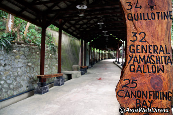
Attraction Places in Penang, Malaysia
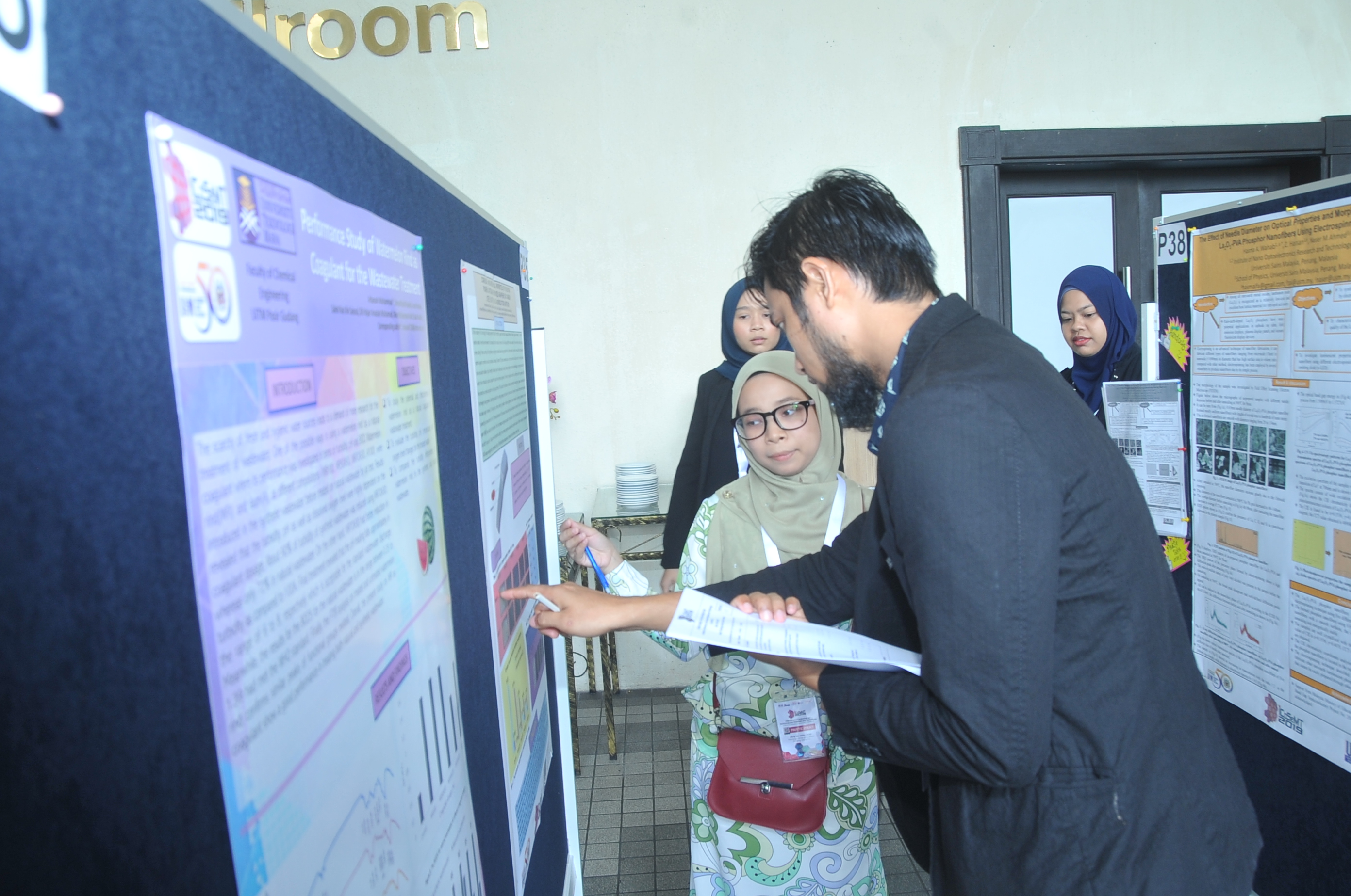
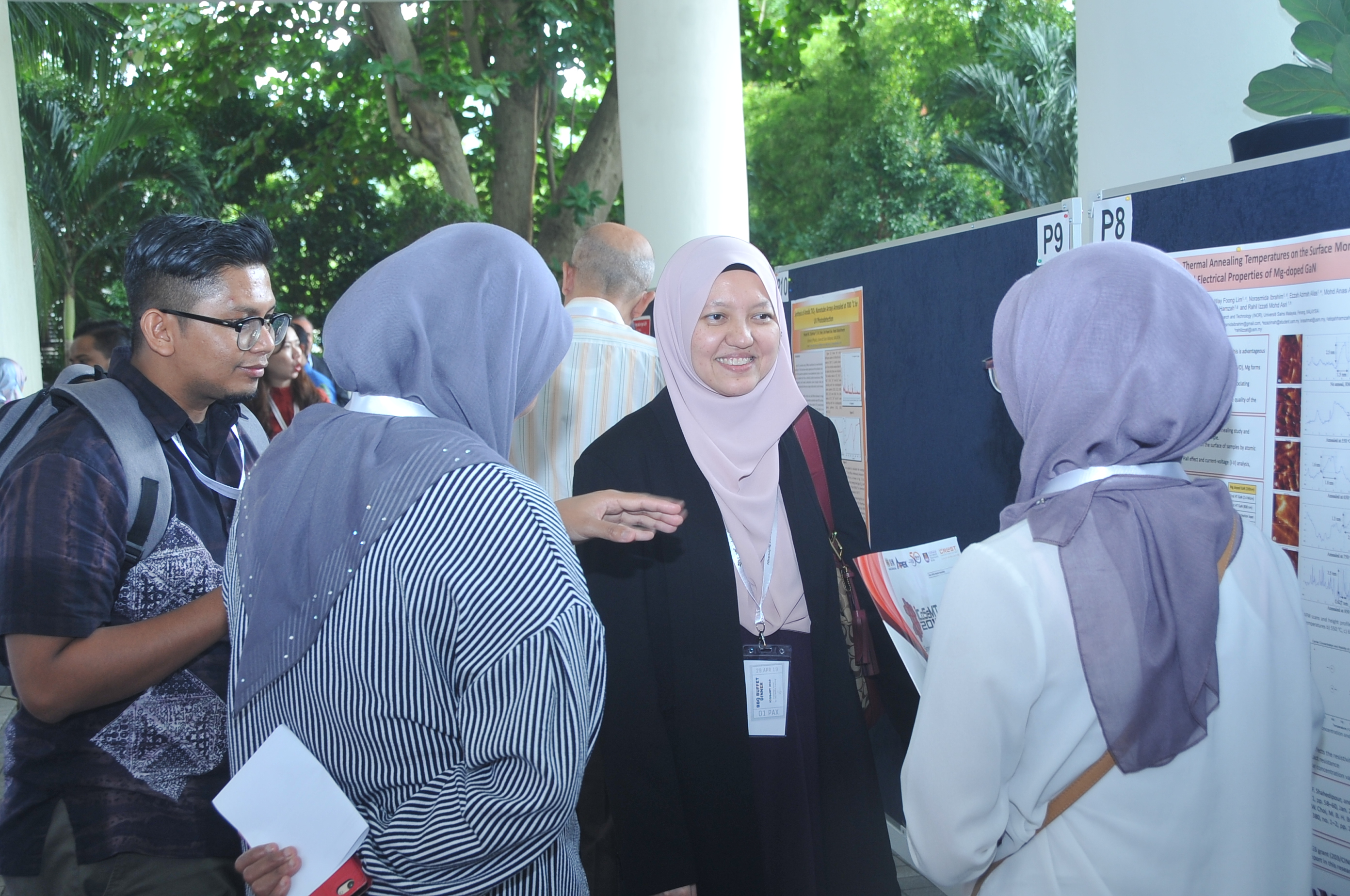
Take a look at our 1st ICoSeMT 2019!
